1. Introduction
Many modern applications contain embedded computing functions and wireless connectivity and these circuits often have highly pulsating load behavior. New generation DC/DC converters will therefore require faster loop response to maintain stable output voltage under the fast fluctuating load conditions. For testing these converters, it is useful to have a tool that can generate similar fast load transients as the final application.
For general DC/DC converters supplying more static loads, fast loop response is not required, and load transient testing would seem not necessary. But applying a fast load step to any voltage regulator will excite the regulation loop over a very wide frequency band, and in some cases will run the control loop to its limits.
Applying a fast load step to any converter and observing the output voltage response during the load step is a quick and easy way to check whether the converter can maintain a well regulated voltage, but it will also highlight potential problems regarding loop stability, input supply stability, slope compensation issues, load regulation and layout problems.
2. Typical DC/DC converter step response
Figure 1 shows an example of a current mode buck converter typical response to a fast 1A load step (VOUT NOM = 3.3V)
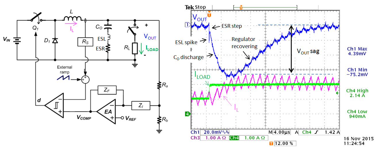
Figure 1: CURRENT MODE CONVERTER FAST LOAD TRANSIENT RESPONSE
The current mode converter cannot react instantly to the load step, so as soon as the load step is applied the output capacitor initially supplies the load. With very fast load steps, the capacitor ESR and ESL will cause a small step and spike, after which the output capacitor starts discharging, causing voltage sag. The output voltage drop is sensed by the error amplifier, which gradually increases VCOMP. This increases the duty-cycle of the switch Q1, and the inductor current will increase to meet the new load demand. The voltage sag and recovery time are determined by the output capacitor, load step amplitude and dI/dt, error amplifier compensation and control loop bandwidth.
Apart from the ESR and ESL spike, the converter step response in this example looks quite smooth, which indicates stable behavior, and the voltage sag is around 75mV which is 2.2%, acceptable for most 3.3V rail supplies. Note that when using low ESR MLCC output capacitors, the ESR step is normally not visible.
There are however several situations that can impact the converter step response shape:
1. Unstable control loop: When the control loop is not well tuned, the converter control can overreact, resulting in bumps or ringing in the output voltage during a fast load step. In severe cases this can lead to oscillation behavior.
2. Unstable input supply: A fast load step on the converter output will also result in a load step on the converter input supply rail. If the input supply is not stable or not well decoupled, input supply ringing may occur, which is transferred to the converter output and looks like control loop instability.
3. Slope compensation issues: Current mode converters use slope compensation to avoid sub-harmonic oscillation in high duty-cycle applications. For slope compensation to work well, a specific amount of inductor ripple current is needed. Incorrect ripple current due to wrong choice of inductor can create unstable sub-harmonic behavior, which can be induced by fast load steps.
4. Duty-cycle limit operation: When the converter is running close to minimum or maximum duty-cycle (i.e. due to critical VIN/VOUT ratio) a fast load step will make the converter hit the duty-cycle limits. This can lead to excessive output voltage undershoot or overshoot, and in some cases can lead to converter protection mode activation.
5. Layout problems: If there is common layout impedance between converter small signal section and the power section, voltage droop or noise coupling may occur, which will worsen during load steps. If the load is some distance from the converter, the increased layout trace resistance will cause a voltage drop when load current is increased, worsening the load regulation properties of the converter. Additionally, the trace inductance can cause ringing at the load during fast load steps.
The following chapters will deal with each of the above cases.
3. Unstable control loop
Loop stability is an important aspect of power converter design. Gain-Phase analysis is the method which is most often used to check loop stability of power converters. However, it is possible to check loop stability via fast load transient tests as well, but it is not always clear how to interpret instability via a step response in order to know what is wrong.
Figure 2 shows a standard current mode buck converter control loop:
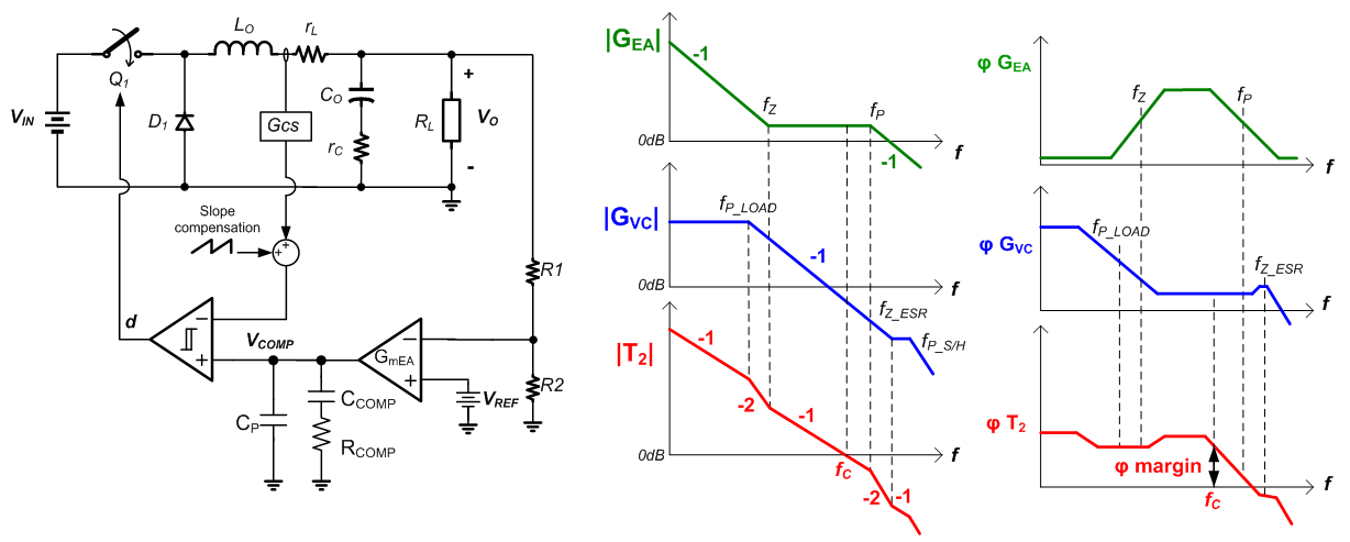
Figure 2
The (simplified) modulator gain GVC has a load pole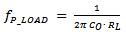 and an ESR zero
The sample and hold effect in the peak current mode control will also result in a double pole at half the switching frequency.
The compensator gain is used to set the converter unity gain frequency fC around 1/10 of the switching frequency to avoid interaction with the double pole:
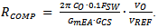 The converter bandwidth is approximated by:
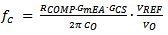
The compensator zero 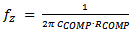 is designed to be close to the modulator load pole
The compensator pole 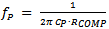 is normally designed to be close to the modulator ESR zero. However, when using MLCC output capacitors, the ESR zero frequency is quite high, often exceeding the switching frequency. In these cases, the compensation pole is set around half the switching frequency to avoid converter switching noise influencing the loop. Note that many power converters ICs have some internal capacitance from COMP to ground, so external CP can be small or omitted.
These guidelines will provide a phase boost around the unity gain frequency, providing sufficient phase margin for stable operation. Unstable operation (insufficient phase margin) can occur when the location of the unity gain frequency shifts, or when the compensator zero & pole frequencies are not chosen correctly.
To illustrate the above theory, let’s examine a typical 12V → 3.3V / 2A application using an 800kHz current mode buck converter with RT7247CHGSP. We can use
Richtek Designer online tool to calculate the required component values for this application as shown in figure 3:
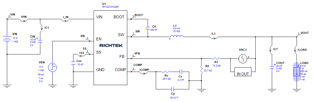
Figure 3
Using the previous formulas and the values from the design tool schematic we get below loop parameters:
fC = 79kHz (close to 1/10 of fSW)
fP_LOAD = 2.2kHz (for 2A load)
Sample and hold double pole fP_S/H = 400kHz
fP_ESR = 1.4MHz (based on two 5mΩ MLCC in parallel)
Compensator zero fZ = 1.8kHz
Compensator pole fP = 508kHz (based on 1pF external + 11pF IC internal capacitance at COMP pin)
The simulated gain-phase plot is shown in figure 4:
The actual bandwidth is 69kHz and phase margin is 57 degrees.
At high frequency, the phase rolls off fast due to the modulator sample and hold double pole.
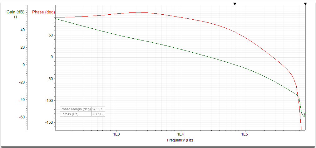
Figure 4
The actual circuit was built with the below component choices.
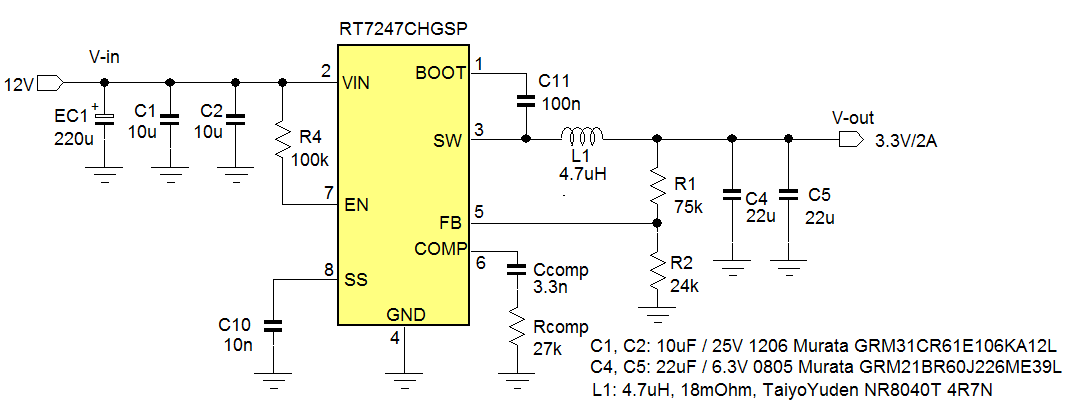
Figure 5
|
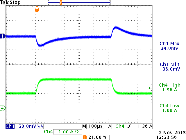
Figure 6
|
When the circuit was tested with a relatively slow load step from electronic load, the step response looked OK.
(see figure 6)
|
But when the circuit was tested with a fast load step (using the fast transient tool described in chapter 8) the circuit response shows excessive ringing, pointing to poor loop stability. See figure 7.
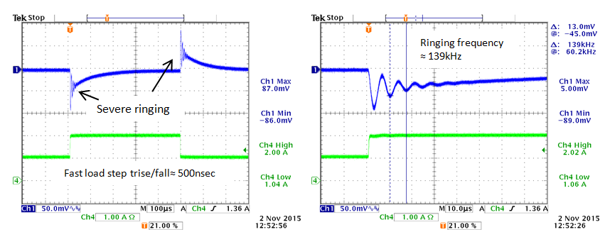
Figure 7
When examining the response in more detail, it can be seen that the ringing shows several cycles, and the ringing frequency is around 139kHz.
|
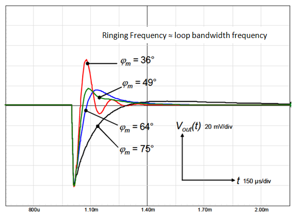
Figure 8: step responses corresponding to different phase margins 1
|
To make an estimate of phase margin, the plot in figure 8 can be used.
(Please note that in our measurements, the ringing waveform is super-imposed onto the exponential recovery waveform which is rather slow due to large CCOMP)
Our measurement shows many ring cycles, and phase margin will be lower than 36o
From the ringing frequency in the step response the loop bandwidth can be derived.
Our measurement shows that the loop bandwidth is very high, around 139kHz.
|
So there is a clear mismatch between calculated loop bandwidth and the actual measured bandwidth.
The parameters that influence loop bandwidth are: 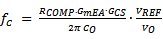
Assuming the IC parameters are correct, the only answer seems that the output capacitor value is not correct.
MLCC capacitors have two important characteristics that influence the capacitance:
1. The DC voltage across the capacitor: higher DC voltage reduces capacitance.
2. The AC voltage across the capacitor: lower AC voltage reduces capacitance.
You should always check your vendor's capacitor datasheet for actual DC bias characteristic and AC voltage characteristic.
In the actual example application we used two 22µF / 6.3V 0805 Murata GRM21BR60J226ME39L in parallel.
We can check the capacitor specifications via the Murata SimSurfing website:
http://ds.murata.com/software/simsurfing/en-us/
The two graphs in figure 9 show the characteristics for the 22µF / 6.3V 0805 GRM21BR60J226ME39L
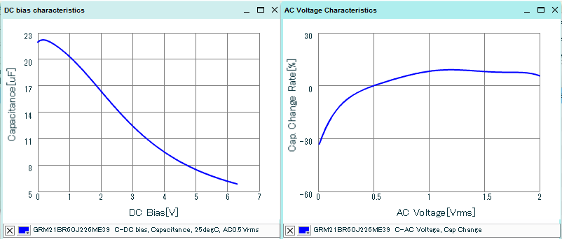
Figure 9
It can be seen that the GRM21BR60J226ME39L capacitance at 3.3Vdc is only 11.4µF and at very low AC ripple (~20mV) it drops a further 30%, so we end up with only 8µF capacitance for each piece, giving a total 16µF output capacitance for the converter, much lower than the original 44µF design value. This low value will increase the bandwidth a lot, resulting in low phase margin.
|
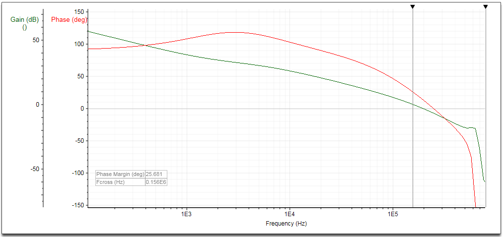
Figure 10
|
Running the Richtek Designer tool again with the actual 16µF output capacitance values confirms this: The loop bandwidth is 156kHz and the phase margin is only 26o.
See figure 10.
|
To solve the instability problem, we need to reduce the bandwidth to the original target value around 80kHz.
This can be done in two ways:
- Increase the output capacitance to get equivalent 44µF total capacitance at 3.3Vdc and low AC ripple.
- Reduce the compensation resistor RCOMP in same ratio as the output capacitance reduction.
|
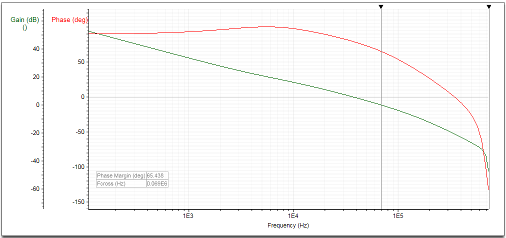
Figure 11
|
Let’s reduce the compensation resistor to reduce loop bandwidth.
No other changes are needed.
The new RCOMP value will be 16/44*26.1k = 9.5k.
We select 9.1k and run the simulation again. The loop bandwidth is now 69kHz and the phase margin is 65o.
See figure 11.
|
The measurement on the actual circuit with this modification shows a smooth step response without ringing.
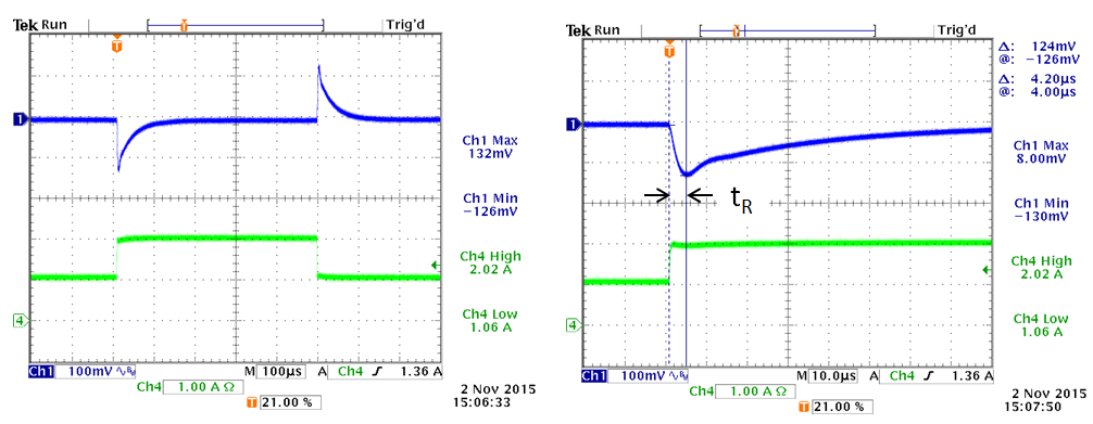
Figure 12
It is interesting to examine the converter response time tR when applying a fast load increase: For current mode converters, tR is inversely proportional to the converter bandwidth and can be used to estimate bandwidth: Practical test show that tR lies between  . In the above example, tR is around 4.2usec, and from this value the converter bandwidth can be estimated to be around 70kHz.
A fast step load measurement can therefore provide information on stability and give an estimation of converter bandwidth, provided that the step-load rise time is much smaller than the converter response time tR.
Too slow load steps like the one using the electronic load box cannot excite the converter loop over a sufficiently wide frequency range, and will not always highlight stability problems. A fast load step with rise time << 1/fC should be used for detecting stability problems in DC/DC converters.
Converter instability due to too small output capacitance can happen with various converter types, including Buck, Boost and LDO, so when using MLCC capacitors in these applications, be sure to check the actual capacitance at the operating conditions. But there are also other cases where converter instability can occur in current mode buck converters, for example when bandwidth is becoming too low: The following example with a buck converter with internal compensation illustrates this.
|
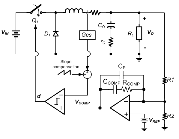
Figure 13
|
Most buck converters with internal compensation use OPAMP type error amplifiers. They behave similar to Gm type error amplifiers with one difference: The error amplifier gain is also dependent on the feedback network impedance.
Loop bandwidth is given by:
Compensation zero is given by: 
Compensation pole is given by: 
|
The example uses
RT7252AZSP, a 340kHz 2A PSM buck converter with internal compensation and PGOOD to make a 5V system and USB supply from 12V input rail. The datasheet recommended components were used to design the circuit.
RT7252AZSP internal parameters: RCOMP = 400kΩ, CCOMP = 35pF, CP = 1pF and GCS = 2.5A/V
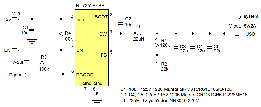
Figure 14
Figure 14 shows the
RT7252A 5V application circuit. The datasheet recommends 44µF total output capacitance. The actual application uses 3x22µF/16V 1206 size MLCC to achieve around 33µF output capacitance at 5Vdc.
For this circuit the following loop parameters can be calculated:
fC = 40kHz (close to 1/10 of fSW)
fP_LOAD = 1.9kHz (for 2A load)
Sample and hold double pole fP_S/H = 170kHz
fP_ESR = 2.5MHz (based on three 5mΩ MLCC in parallel)
Compensator pole fP = 398kHz
Compensator zero fZ = 11kHz (the compensator zero frequency lies relatively high due to the maximum capacitance that can be realized inside an IC)
|

Figure 15
|
Applying a fast step load to this circuit shows a smooth response; the circuit is fully stable.
From the response time tR, the converter bandwidth is estimated to be around 41kHz.
|
It was found that USB hot-plug events result in rather large 5V supply voltage dips. To reduce the voltage dip during USB hot-plug, a 150µF low ESR polymer capacitor was added to the 5V output rail, see figure 16.
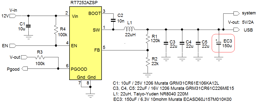
Figure 16
|
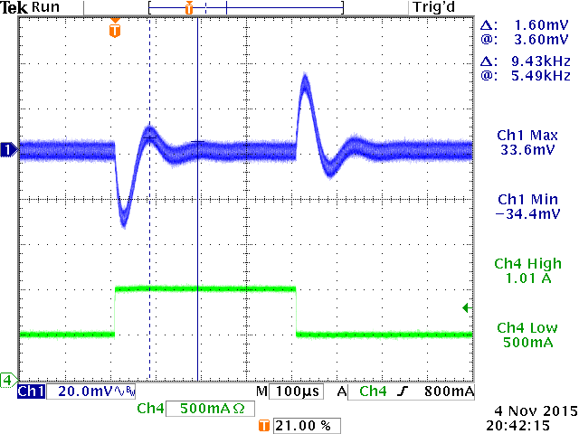
Figure 17
|
Stability was again checked via a fast step load:
Now the converter shows a step load response with ringing, indicating insufficient stability.
The ringing frequency was measured to be around 9.4kHz, pointing to a low loop bandwidth frequency.
This low bandwidth can be explained by the larger output capacitance value: 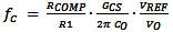
which results in around 7.3kHz bandwidth when the 150µF extra output capacitance is added.
|
|
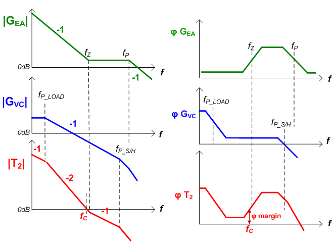
Figure 18
|
The poor stability can now be explained:
The extra output capacitance reduces the bandwidth and also reduces the converter load pole. The internal 11kHz compensation zero now lies above the 9.4kHz unity gain frequency.
The low frequency load pole causes phase to drop quickly, and the loop crosses 0dB before the compensation phase boost has taken effect, resulting in low phase margin at the 0dB frequency.
|
To improve the phase margin, it is best to set the converter unity gain frequency well above the compensator zero frequency to let fC fall inside the phase boost region. This can be done by increasing the error amplifier gain by reducing R1. To set the bandwidth back to around 34kHz, R1 needs to be reduced with a ratio of 9.4/34, so R1 becomes 33kΩ. Of course R2 needs to be reduced as well to maintain the 5V regulation voltage.
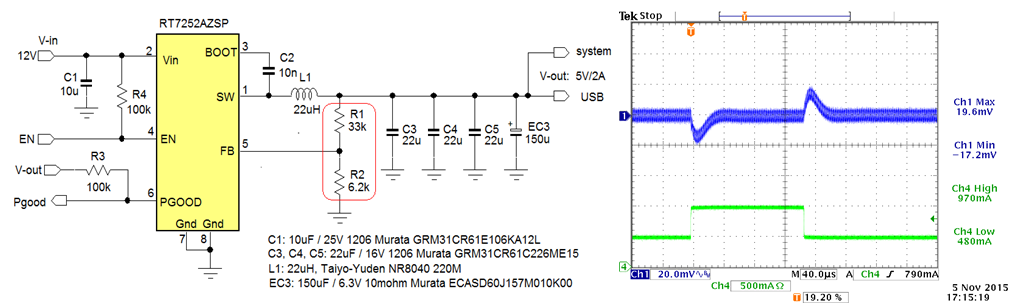
Figure 19
Step load test with this modification confirms that the circuit is stable. Bandwidth is around 35kHz.
See figure 19.
Above stability examples are related to current mode control topology buck converters.
ACOT control topology buck converters do not include error amplifiers, and are easier to use, but in some cases can show under-damped step load response. For more information on stability of ACOT devices, please read the application note ACOT Stability Testing.
4. Unstable input supply
In the previous chapter, fast load transients were applied to a DC/DC converter output and the output voltage was observed for ringing which could indicate unstable converter loop. In some cases, ringing at the converter output does not always mean loop instability. A load step at converter output will also result in a load step at the converter input. The speed of the input supply load step depends on the speed of the converter itself, so very fast converters will transfer almost the full step load speed to the converter input supply. Any instability or resonance at the input supply will then result in ringing on the input rail. Depending on the DC/DC converter line regulation capability, the input supply ringing will be (partly) visible on the converter output as well, and could lead to incorrect conclusions on converter stability.
A practical example can illustrate this effect:
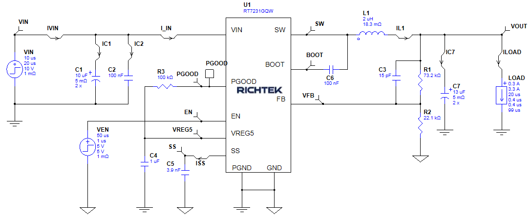
Figure 20
Figure 20 shows
RT7231GQW, a fast 18V/4A 700kHz ACOT part in a 10V input to 3.3V output rail. Richtek Designer is used to analyze the design. The output capacitance is modified to 2x 13µF to include the DC bias effect of two 22µF/16V 1206 size MLCC capacitors at 3.3Vdc. The analyzer step load is modified to create fast 400nsec 3A load steps.
|
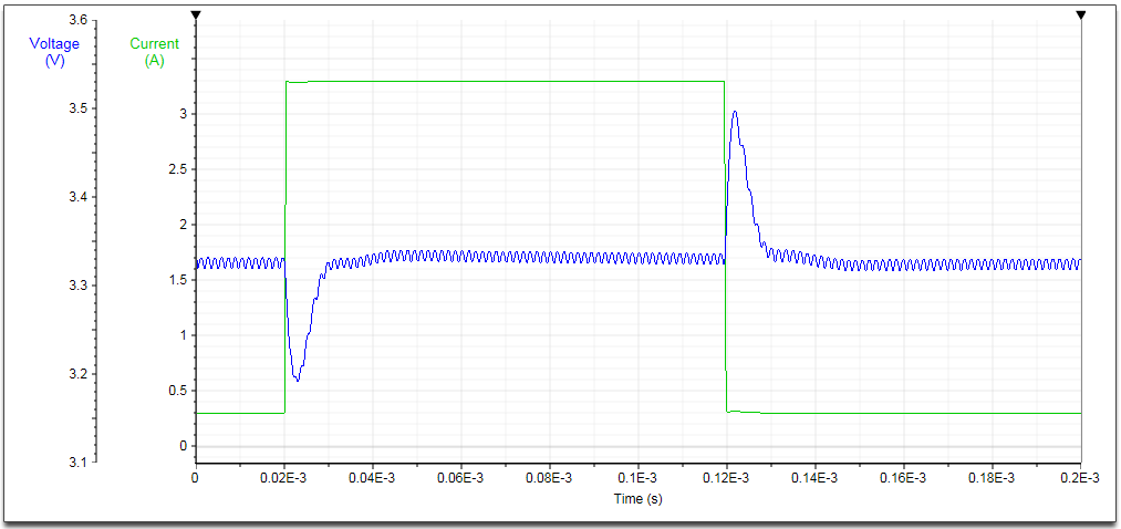
Figure 21
|
The design tool transient analysis shows smooth step load response, so the circuit shows good stability.
See figure 21.
|
|
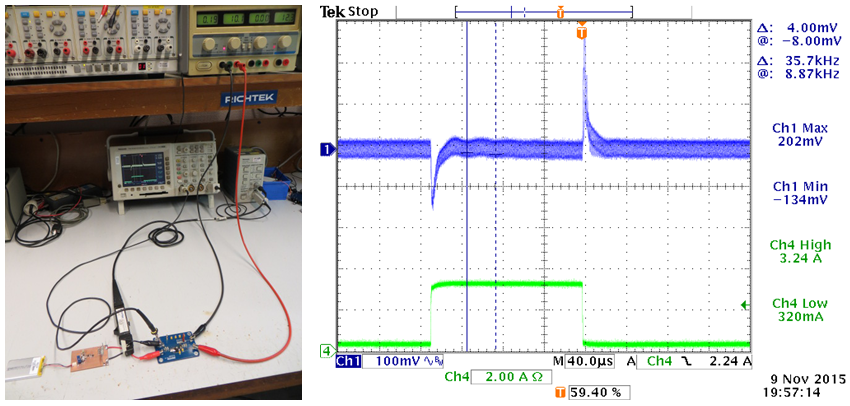
Figure 22
|
When the same circuit was tested in the lab powered by a lab supply and using the fast transient tool as described in chapter 8, there was some slight ringing visible in the later part of the step load response with a frequency of around 36kHz, See figure 22.
Component values were double-checked, but there was no reason found for any converter instability.
|
|
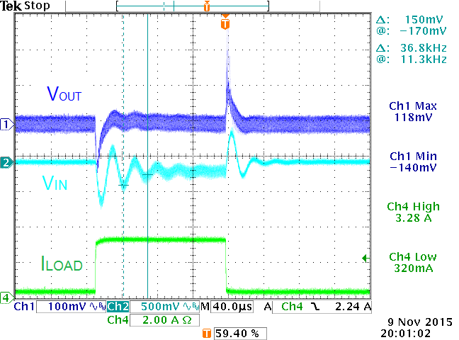
Figure 23
|
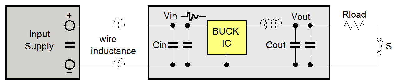
When measuring the voltage on the converter input capacitors, it was found that there was considerable ringing on the input voltage rail with the same ringing frequency as was seen on the converter output.
This input ringing is caused by the resonance of the low ESR ceramic input capacitors and the inductance of the input supply leads and lab supply.
|
|
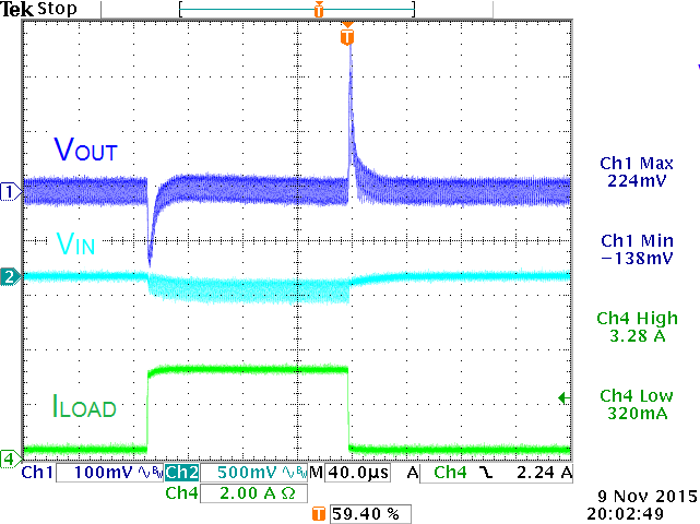
Figure 24
|
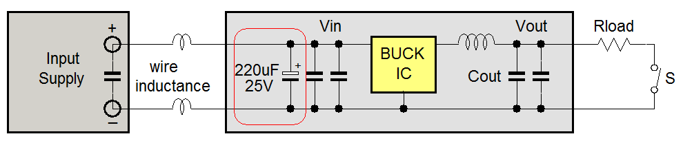
In this case the input supply ringing is easily solved by adding an electrolytic capacitor in parallel with the buck converter input capacitors. Electrolytic capacitors have rather high ESR and they therefore act as an RC snubber, which effectively damps the resonance of the ceramic input capacitors with wire/trace inductance. Normally 220µF/25V electrolytic capacitors with ESR around 50~100mΩ are sufficient. They will also suppress input voltage spikes due to hot-plug event of live input supplies.
|
When doing fast transient testing on converters, it is highly recommended to add a 220µF/25V or larger electrolytic capacitor in parallel with the ceramic input capacitors to avoid the possibility of input ringing which could transfer to converter output and be mistaken for converter instability.
5. Slope compensation issues
Current mode buck converters use slope compensation to avoid sub-harmonic switching behavior in high duty-cycle applications; an internal ramp is added to the current sense waveform and then compared to the error amplifier output.
|
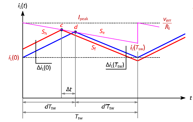
Figure 25 1
|
For slope compensation to work well, the slope compensation slope Se needs to be at least a certain ratio of the sensed inductor current down-ramping slope Sf as shown in figure 25
In theory, Se needs to be ≥ 0.5 Sf, but in practice, the internal ramp slope is often larger than this, to guarantee sufficient slope compensation in a wider range of applications and component values.
The sensed inductor current down ramping slope Sf is determined by VOUT/L and the IC current sense gain GCS and therefore L needs to have a certain value at certain VOUT to meet the requirement with the IC internal slope compensation ramp.
|
Incorrect inductor current slope due to wrong choice of inductor value can create problems.
The inductor value in general DC/DC switching converters is often calculated to achieve an inductor ripple current with certain percentage of the maximum load current, usually around 30%. But this will not always give the best results. The following examples will illustrate this.
For an industrial application we need to derive a 5V/5A rail from a supply with minimum 6V input voltage. This requires a high current buck converter with high duty-cycle capability. For this application we select RT2856GQW, an industrial grade 6A current mode part with low Rdson MOSFETs and close to 100% duty-cycle capability. See figure 26.
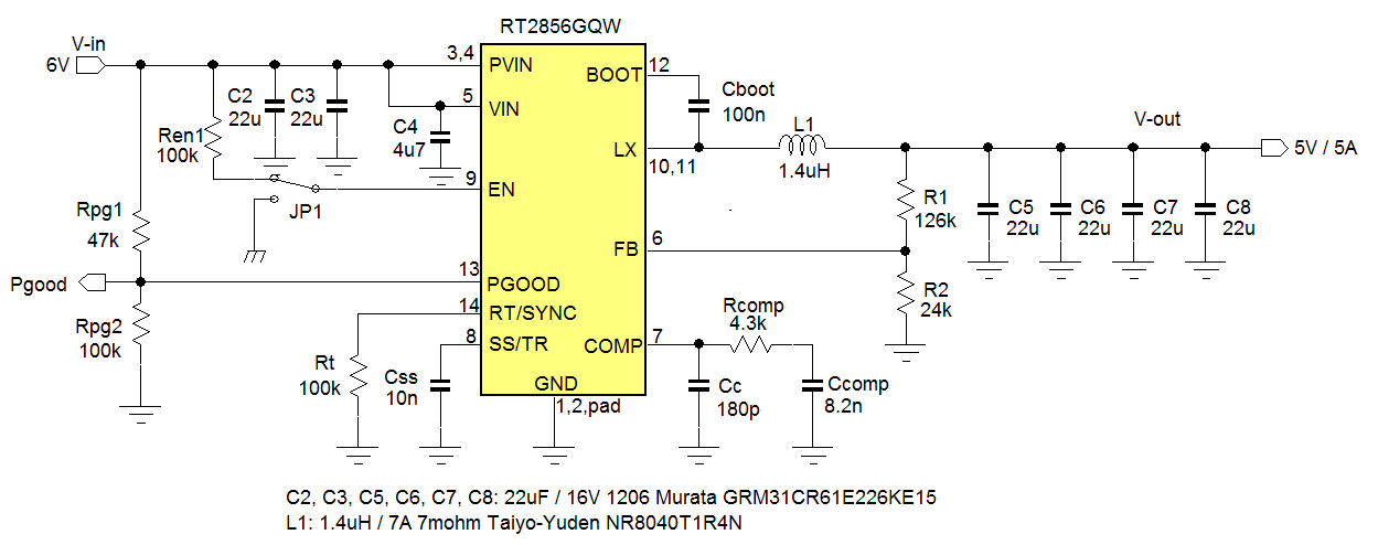
Figure 26
Most component values are taken from the recommended values from datasheet. 4 pieces of 22µF/16V GRM31CR61E226KE15 MLCC were used to achieve the recommended 44µF output capacitance at 5Vdc bias.
The inductor value was calculated to give a current ripple of around 0.3*ILOAD_MAX based on the formula
 VIN = 6V, VOUT = 5V, f = 500kHz, ΔIL = 0.3*5A = 1.5A, L = 1.11µH, choose 1.4µH.
When this circuit was tested with a fast load step, the output voltage showed increased ripple after the step load. See figure 27.
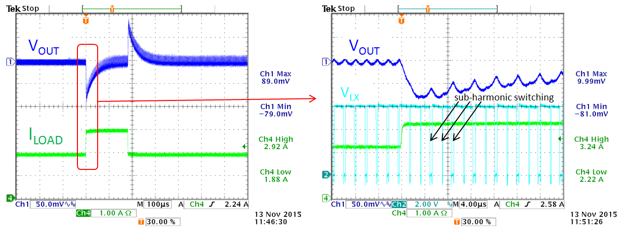
Figure 27
After zooming in and adding the switching voltage, it can be seen that the step load seems to induce irregular duty-cycle with a repetition rate of ½ fSW. This indicates sub-harmonic oscillation which is related to slope compensation. After more experiments, it was found that the sub-harmonic oscillation will occur at higher load levels and lowest VIN.
The sub-harmonic oscillation in this application can be explained: As mentioned previously, the IC internal slope compensation ramp Se is designed for certain inductor current falling slope ramp Sf. The inductor current down ramping slope Sf is determined by VOUT/L. When VOUT increases, L must increase as well to keep the falling slope Sf matched to compensation slope Se. This can be seen from the datasheet recommended inductor values: L increases at higher VOUT. In this application example, the inductor value was based on 30% ripple of 5A application current (1.5A) but due to the fact that the application VIN is close to VOUT, a small inductor value is needed to generate this 1.5A ripple current. The small inductor value results in a very steep inductor current falling slope Sf, and the IC internal slope compensation ramp Se is insufficient to meet the criteria for avoiding sub-harmonic oscillation in high duty-cycle application.
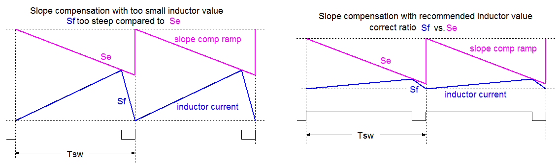
Figure 28
|
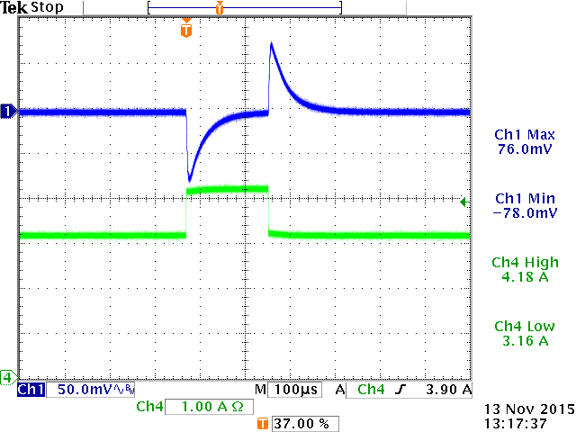
Figure 29
|
The solution in this case is to increase the inductor value to be more in line with the datasheet recommended value of 4.7µH for 5V application. To avoid too large body size inductor, it is allowed to use slightly lower than 4.7µH, but don’t deviate too much. In this case a 3.3µH inductor was selected, which solved the sub-harmonic instability over the full input voltage and load range, see figure 28.
This effect can also be simulated with the
Richtek Designer simulation tool.
|
For another example where wrong inductor value selection can lead to problems, let’s check a step-down application from 15V input to 3.3V output, 0.5A maximum load current. For this design RT7247CHGSP (18V, 800kHz 2A current mode buck converter) was chosen, see figure 30.
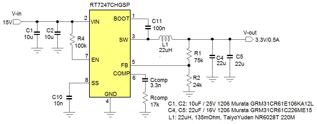
Figure 30
Most component values are taken from the recommended values from datasheet.
The inductor value was calculated to give a current ripple of around 0.3*ILOAD_MAX based on the formula
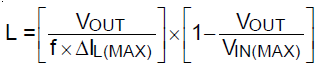 VIN = 15V, VOUT = 3.3V, f = 800kHz, ΔIL = 0.3*0.5A = 0.15A, L = 21.5µH, choose 22µH.
When this circuit was tested with a fast load step, the response showed some ringing, indicating low phase margin.
|
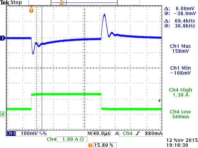
Figure 31
|
When calculating the circuit loop parameters
(using Co = 2x17µF due to 3.3Vdc bias)
fC = 67kHz, which matches the measured ringing frequency.
fP_LOAD = 710Hz (for 0.5A load)
Sample and hold double pole fP_S/H = 400kHz
fP_ESR = 1.9MHz (based on three 5mΩ MLCC in parallel)
Compensator pole fP = 851kHz (based on 11pF internal CP capacitance)
Compensator zero fZ = 2.84kHz
|
Based on the calculated values, the unity gain frequency seems correct, and is less than 1/10 of fSW. Compensation zero frequency lies well below the unity gain frequency, and compensator pole is close to fSW. From these values, there is no clear reason to expect low phase margin.
However, the inductor value is much higher than the recommended value of 4.7µH for 3.3V output, because the 30% ripple was calculated as a ratio of the rather low maximum application load current of 0.5A.
The high inductor value will result in a very small inductor current ripple compared to the slope comp ramp amplitude which was designed for an inductor ripple of 30% of the IC maximum current rating of 2A.
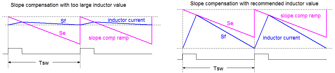
Figure 32
Figure 32 shows the ratios of inductor current ripple vs. slope comp amplitude with different inductors.
Too large inductor values result in very small current ripple amplitude compared to the slope compensation ramp amplitude. In these cases, peak current mode control starts to behave like voltage mode control, which requires different compensation compared to peak current mode control. What happens in the frequency domain is that the modulator double pole moves from ½ fSW towards fC. This results in faster modulator phase roll-off. The phase boost around fC will be insufficient, resulting in lower phase margin.
For this case, the phase margin can be increased in several ways:
1. Calculate the inductor value for a 30% current ripple of the IC maximum rated current. For low current applications, it means that the inductor value will be lower, and the current ripple will be relatively big compared to the application current.
2. Reduce the converter bandwidth; in this case setting the bandwidth around 1/20 of fSW will provide sufficient phase margin.
3. Add type III compensation by adding a feed-forward capacitor CFF across R1. The value can be estimated by:  . This will add extra phase boost around the unity gain frequency.
|
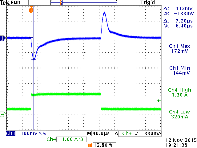
Figure 33
|
The circuit was tested after adding solution b: Reducing the bandwidth to 40kHz by reducing RCOMP to 8.2k. The converter now shows stable step response, measured bandwidth around 41kHz, see figure 33.
These results can also be verified by using
Richtek Designer simulation tool.
|
It should be noted that in most low duty-cycle applications, it is better not to use inductor values that are much larger than recommended values, because very small current ripple will also make the converter duty-cycle more noise sensitive, leading to jitter. Additionally, larger inductor values often require larger body size inductors, which are more expensive.
6. Layout problems
Layout plays an important role in DC/DC converter design. Layout becomes even more critical in applications that exhibit very fast load transients, like VCORE, DDR memory and other high dI/dt load behavior, especially when the load itself is sensitive to supply voltage variations. Physical distance between converter and load can be a limiting factor in the quality of the supply voltage under dynamic load, so in these cases it is important that the DC/DC converter is placed as close as possible to the load point. If this is not possible, the trace resistance and inductance between converter and load will impact the dynamic and static load regulation considerably.
A practical example can highlight this:
|
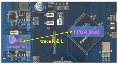
Figure 34
|
In the board shown in figure 34, the buck converter is some distance away from the FPGA load. Depending on the layout of the supply copper planes and ground plane, there will be some parasitic resistance and inductance between the converter and load.
This parasitic impedance will result in voltage drop when static and dynamic loads occur.
|
In the 12V to 1.0V/5A example shown in figure 35,
RT7239GQW ACOT buck converter regulates the output voltage locally, and the distance between the converter and 1V/5A load is shown having inductance and resistance.
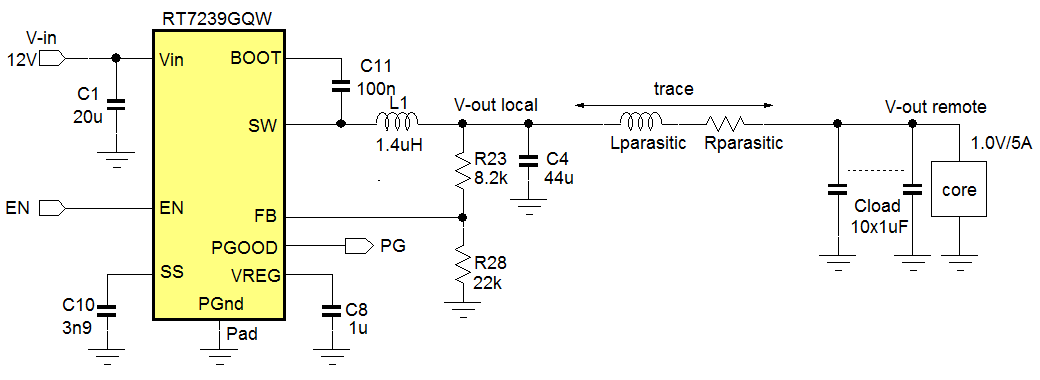
Figure 35
|
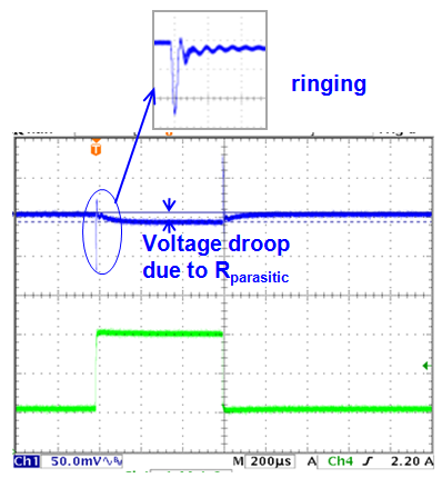
Figure 36
|
When a high current load occurs at the load, the voltage at the load will show a static drop due to the trace resistance, resulting in poor load regulation.
The fast load step dI/dt will also cause the parasitic trace inductance to resonate with the capacitance at the load, resulting in a high frequency ringing at the load. So this ringing is not converter instability, but a layout related artefact.
To reduce the supply variations due to trace resistance and inductance, different solutions need to be incorporated.
|
The voltage droop due to trace resistance can be solved by applying remote sense. The converter voltage sense should be moved from the local VOUT position to the VOUT position at the load, by connecting R23 to the load remote sense load point. But the parasitic trace inductance together with the capacitance at the load will result in some phase shift at higher frequency. This extra phase shift in the feedback loop may cause converter instability. To avoid instability an extra local high frequency feedback element is added by means of C30 as shown in figure 37.
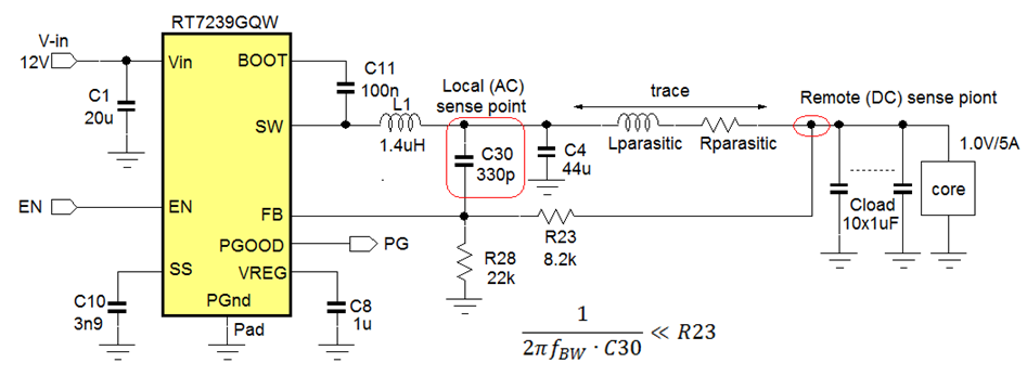
Figure 37: remote sense with separate high frequency and low frequency sense points
The value of C30 should be such that its impedance at the converter unity gain frequency is much lower than the remote sense resistor R23: 
|
Figure 38
|
When the converter FB pin is sensitive to noise, the configuration as shown in figure 37 can be used: An extra remote DC sense resistor and local AC sense capacitor are added, making sure the capacitor impedance is lower than the resistor at converter loop bandwidth frequency.
See figure 38.
|
|
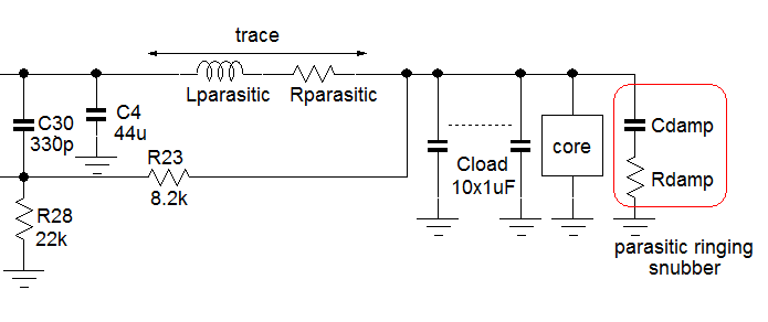
Figure 39
|
To reduce the ringing at load side due to parasitic inductance, an RC snubber can be added at load side to damp the ringing.
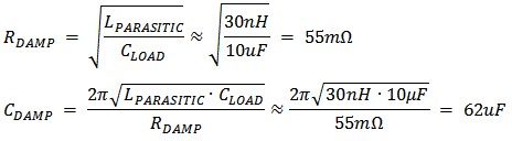
To determine the RC snubber values, the ringing frequency has to be measured and from the ringing frequency, the parasitic inductance can be derived.
 LPARASITIC was found to be 30nH. LPARASITIC was found to be 30nH.
|
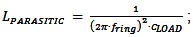
Now the RC snubber resistance and capacitance can be calculated:
|
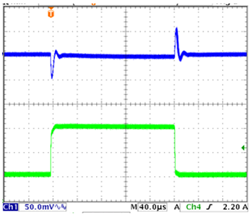
Figure 40
|
In practice adding a suitable electrolytic or polymer capacitor at load side with capacitance and ESR similar to calculated values can be used to damp the layout ringing. Figure 40 shows the fast step load results at load side after remote sense and damping network were added.
|
7. Summary / Practical tips
Check converter output capacitance
In many DC/DC converters, the output capacitance plays an important role in the loop stability. When using MLCC capacitors, always consider the DC bias and AC ripple effects on the capacitance value. When making changes to the output capacitance, double check loop stability.
Sufficient Step load speed
Make sure the load transient is fast enough to excite the loop over a sufficiently wide frequency range. Load step rise time should be much lower than 1/fC.
The load step amplitude is not so critical when checking for converter problems, but it is better to use a smaller load step (i.e. 20~30% of max load current) and vary the DC (static) current level of the load step over the full application range. In this way, converter behavior over the full load range can be checked.
Ensure stable input supply
When load step response shows ringing, it should be checked whether the ringing is caused by the converter itself or input supply ringing. When doing fast load steps, always add an electrolytic capacitor in parallel with the input supply decoupling capacitors close to the converter.
Correct inductor value
Choosing a too large or too small inductor can lead to problems. In low duty-cycle applications, inductor ripple should be calculated based on a percentage of the IC rated current. In high duty-cycle applications, consider the inductor falling slope in relation to the IC internal slope compensation slope. IC recommended inductor values at different VOUT can serve as a guideline.
Low impedance between converter output and load
In applications where the load shows very fast load transients, the DC/DC converter should be placed as close to the load as possible. Keep the tracks between converter and load as wide as possible, and ensure a solid ground plane for return currents. Use remote sense when load regulation problems occur, but always check the converter stability directly at the converter output when applying remote sense. Use local AC feedback for remote sense applications when converter shows instability. Add RC snubber or polymer capacitors to damp layout induced ringing.
Duty-cycle limit and step-load timing
Fast load transients can result in big changes in the converter duty-cycle. In some cases it can lead to the converter reaching its minimum or maximum duty-cycle limit. The timing of the load step in relation to the converter switching cycle can also influence the load step response.
Let’s show this with the below example where a RT7294CGJ6F, a 18V/2.5A ACOT buck IC in SOT-23-6 package is used to make a cost effective 1V core supply rail:
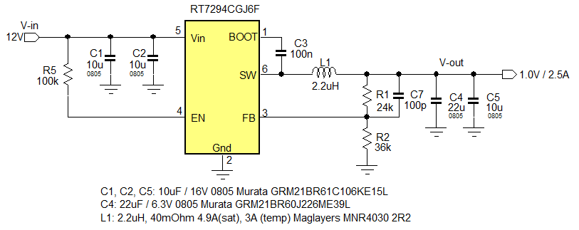
Figure 41
ACOT converters have a fixed ON time and a variable OFF time and can react very fast to sudden load changes. The converter maximum duty-cycle is limited by the ON time together with the minimum OFF time that the converter can achieve. ACOT converters can also achieve very low duty-cycles, down to 0%; when a fast high to low load step occurs, the ACOT converter will keep the low-side MOSFET on continuously to ramp the inductor current down as fast as possible, temporarily reducing the duty-cycle to 0%. Figure 42 shows this effect.
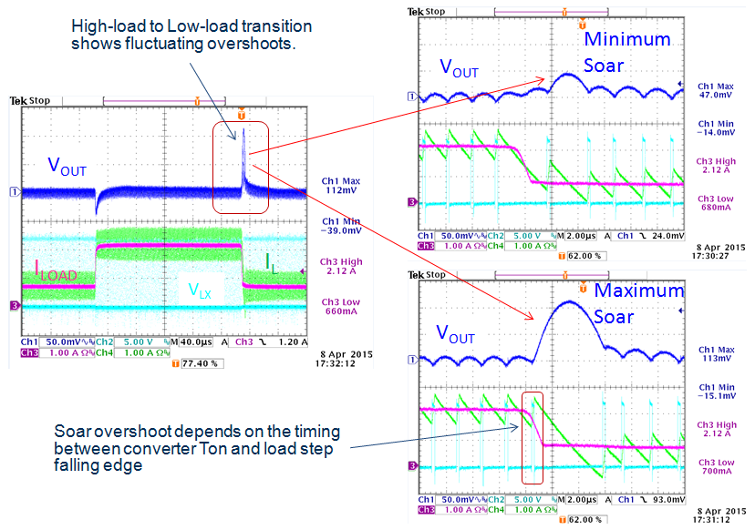
Figure 42
The overshoot during high-low load transient is called output voltage soar. As can be seen in this example, the voltage soar is not constant. If the load step occurs during the converter OFF time, the inductor current is already ramping down and the converter simply keeps the low-side MOSFET on to continue this down-ramping. But when the load step occurs just when the converter is initiating a (fixed) ON time, it has to wait until the ON time has passed before inductor current down-ramping can start. This causes a larger voltage soar. The fluctuating voltage soar that can be seen with repetitive load steps should not be mistaken for converter instability.
Step load difference between PSM and Force-PWM converters.
Some DC/DC converters have enhanced light load efficiency by means of PSM (Pulse Skipping Mode, sometimes also called PFM or Discontinuous Mode). These parts will inhibit the low-side MOSFET switch-on when inductor current goes negative, and will reduce switching frequency at very low load current. The average output voltage when the converter is operating in PSM mode is normally slightly higher than when working in CCM (Continuous Conduction Mode). Due to this effect the output voltage response may show worse load regulation when the converter changes from PSM to CCM operation during a load step. Additionally, a high-load to low-load transition may show a longer voltage soar because a PSM converter cannot sink any current. The above phenomenon is illustrated with the example below: RT7272A and RT7272B are 36V/3A 500kHz buck converters for industrial applications. RT7272A is a force-PWM part and RT7272B is a PSM part. Both are tested in the same 24V to 3.3V/2A application, as shown in figure 43.
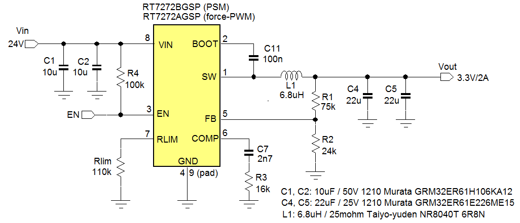
Figure 43
The difference between the PSM and force-PWM parts during load steps is shown in figure 44.
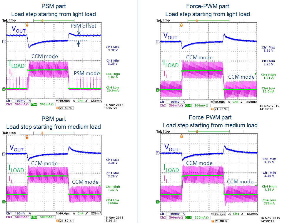
Figure 44
PSM parts will show a PSM offset when the load step starts in PSM mode and ends in CCM.
(The PSM offset is normally around 1% of VOUT)
Force-PWM parts will always stay in CCM regardless the load condition. At light load, inductor current of force-PWM parts will go negative.
When the load step starts from medium load where inductor current minimum value is just above zero, the step loads of both PSM parts and force-PWM parts will be the same, as the converters always stay in CCM.
Applications requiring tight load regulation and good transient response over the full load range should use force-PWM parts. For applications that require very good light load efficiency you should select PSM parts. Many Richtek buck converters are available in pin compatible PSM and force-PWM versions. Some parts have a mode selection pin to set the part in PSM mode or force-PWM mode.
8. Fast load transient tool
Most electronic loads can generate load steps, but often the load step dI/dt that the generator can achieve is limited. This is partly due to electronic load internal circuit limitation, but also due to the inductance of the relatively long wires from electronic load box to application.
To generate fast load steps, a simple DIY tool can be used where a MOSFET switches a load resistor on and off.
Figure 45 shows the basic principle of the fast transient tool: a pulse generator switches a MOSFET on and off. The switching speed of the MOSFET can be adjusted by an optional RC network in the gate drive. The MOSFET drain connects to a resistor R2 which can be chosen for certain dynamic load step amplitude. A resistor R1 sets the static low level of the load step. The load current step can be measured via a current probe, and the converter output voltage should be measured directly across the output capacitor or application load point.
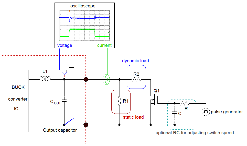
Figure 45
A practical solution for a flexible fast transient tool is shown in the schematic in figure 46:
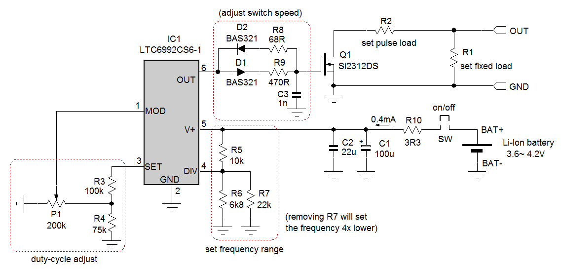
Figure 46: schematic of fast load transient tool
IC1 is a voltage controlled PWM generator IC. The voltage on the MOD pin sets the PWM duty-cycle, the voltage on the DIV pin sets the frequency range, and the resistor value connected to the SET pin sets the precise frequency. The OUT pin has sufficient driving capability to drive small MOSFETs with fast rise and fall times. The duty-cycle is normally set at a low level, around 5%. This makes it possible to draw larger pulse currents while limiting the total power in the pulse load resistor and MOSFET. A pulse width of around 150usec is sufficient to see the full voltage sag and recovery in most DC/DC converters, so the PWM frequency can be set at around 330Hz. The LTC6992 datasheet recommends a 1024 clock frequency divider for this frequency which can be achieved via a divider ratio of 0.344 via R5 and R6//R7.
The frequency is finally set by R3+R4//P1 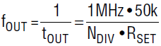 which results in 316Hz with given values.
0.1VSET ~ 0.9VSET on the MOD pin gives 0% ~ 100% duty-cycle adjustment range. With the given values for R3, R4 and P1, the duty-cycle adjustment range is 0 ~ 35% by adjusting P1.
The LTC6992 OUT pin has fast transient speed and current capability of ±20mA, which is sufficient to switch on/off Q1 MOSFET Si2312DS within 100nsec. Most applications don’t need this speed, and by means the network D1, D2, R8, R9 and C3, the rise and fall times of the pulse current can be tuned. With given values, the rise and fall times will be around 400nsec, which is sufficient to see stability or layout effects in most DC/DC converter applications. For the given Si2312DS MOSFET, pulse currents up to around 8A can be used. Higher currents are possible, but the Rdson voltage drop needs to be considered for the pulse load resistor. Especially with low voltage supplies, a lower Rdson MOSFET with low QG may be selected.
It is most convenient to power the circuit via a Li-Ion battery; this makes the circuit fully isolated and avoids ground bounce between grounded equipment. The circuit is designed in such a way that battery voltage variations will not impact frequency or duty-cycle settings, and with a current consumption of only 0.4mA, the battery life is very long.
Figure 47 shows a possible layout for the circuit.
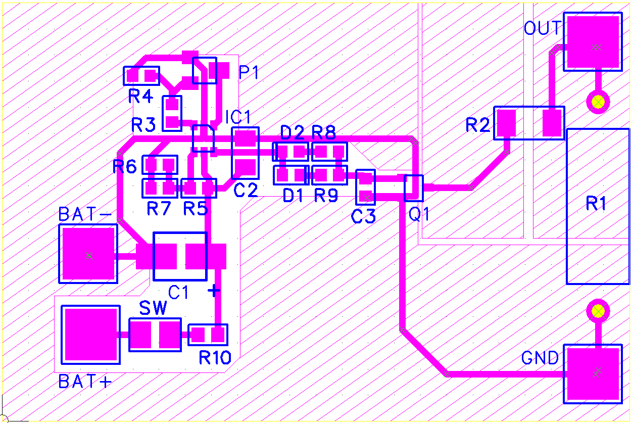
Figure 47: layout of fast load transient tool
It is important that the impedance path of the load to MOSFET is low. A copper plane is reserved for soldering multiple pulse load resistors in parallel. The static load resistor can be a fixed or variable power resistor.
|
Item
|
Value
|
Type or Part number
|
|
R1
|
1Ω ~ 25Ω fixed or variable power resistor
|
Leaded 10W or Rheostat variable 25W
|
|
R2
|
SMD power resistors 1Ω ~ 10Ω 0.25W/0.75W/2W
|
1206 0.25W / 1210 0.75W / 2512 2W
|
|
R3
|
100k 1% 0.1W
|
0603
|
|
R4
|
75k 1% 0.1W
|
0603
|
|
R5
|
10k 1% 0.1W
|
0603
|
|
R6
|
6.8k 1% 0.1W
|
0603
|
|
R7
|
22k 1% 0.1W
|
0603
|
|
R8
|
68R 1% 0.1W
|
0603
|
|
R9
|
470R 1% 0.1W
|
0603
|
|
R10
|
3.3R 1% 0.1W
|
0603
|
|
P1
|
200K TRIMMER, 5 TURN SMD
|
Bourns 3214W-1-204E
|
|
C1
|
100µF/10V 6.3X5.2 electrolytic capacitor SMD
|
Panasonic MCESL10V107M6.3X5.2
|
|
C2
|
22µF/16V 1206 X5R
|
Murata GRM31CR61C226KE15L
|
|
C3
|
1nF/50V X7R
|
0603
|
|
D1, D2
|
200V/200mA fast diode SOD323
|
NXP BAS321
|
|
SW
|
Jumper header + jumper 1ROW, 2.54MM
|
MOLEX 90120-0126
|
|
Q1
|
20V / 33mΩ Rdson N-MOSFET SOT23-3
|
Vishay Si2312DS
|
|
IC1
|
Voltage controlled PWM generator, SOT-23-6
|
Lineartech LTC6992CS6-1#TRMPBF
|
|
Battery
|
3.7V nom. 1250mAh Li-Ion battery
|
Varta PLF503759.06.8080/2528F or similar
|
Because the circuit is simple, it is also possible to build the components on a copper board by means of isolation routing: copper is removed from a copper clad board with a fine engraving tool to obtain a layout similar as the example. Figure 48 below shows the required components and the hand-cut PCB.
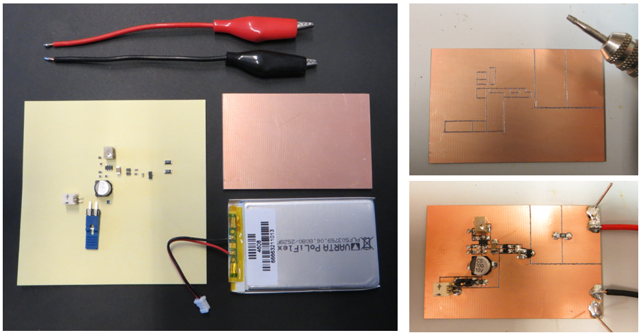
Figure 48
The final tool will look like figure 49:
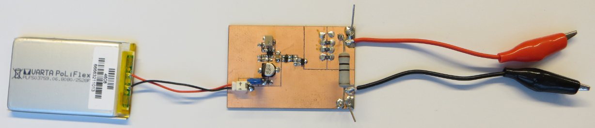
Figure 49
Measuring the load step current is most convenient by means of a current probe hooked into one of the leads of the load transient board. The advantage of a current probe is that it is isolated, so it will not add ground loops to the measuring system. But the current probe can add some extra inductance in the load step circuit which can affect step current shape when rise and fall times are very fast; (~100nsec). However, not all current probes have sufficient bandwidth to measure very fast rise and fall times.
It is also possible to measure current by means of a current sense resistor in the system as shown in figure 50.
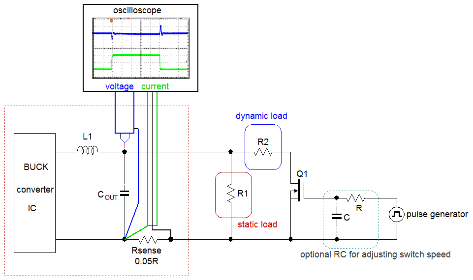
Figure 50
If the scope channels share a common ground, it is absolutely necessary to connect the sense resistor ground to the same ground point as the voltage probe ground. Even small impedance between these points will result in voltage differences between the current and voltage probe grounds, and the voltage waveform on the scope will be affected. This can easily be tested by triggering on the voltage waveform and connecting / disconnecting the current sense connector from the scope. If the voltage waveform changes, there is ground current.
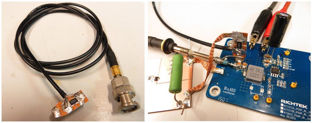
Figure 51: current measurement via sense resistor.
The pictures in figure 51 show the current sense jig and measurement setup when using very fast rise and fall times. It is best to terminate the current sense cable into 50Ω at the scope to avoid ringing due to cable reflections. Note that this will slightly attenuate the current sense. Figure 52 shows an ultra-fast load step measurement using the current sense resistor tool. (scope probe attenuation was adjusted for correct current reading)
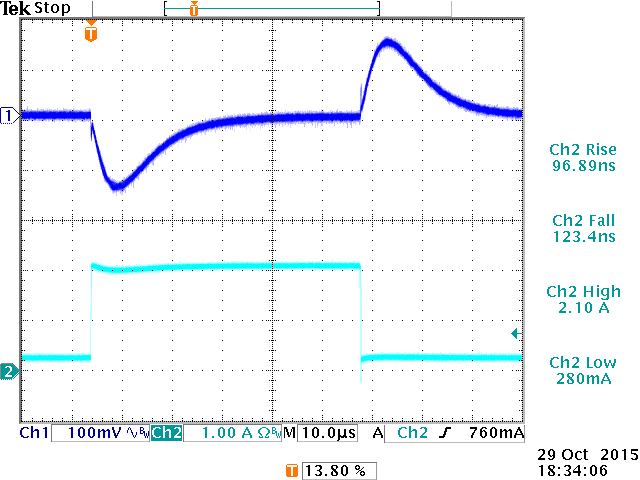
Figure 52: ultra fast load step using sense resistor for current measurement.
9. Richtek Load Transient Tool
Richtek has developed a Load Transient Tool based on the same principle as the DIY tool described in chapter 8.
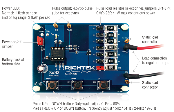
Figure 53: Richtek load transient tool functionality
The Richtek Load Transient Tool contains a
micro controller that switches a MOSFET on and off with a certain duty-cycle.
By means of jumpers, 7 different pulse load resistors can be selected. The tool
includes an adjustable 10Ω power resistor for setting the static load level. This
tool can generate very fast load steps (~500nsec rise/fall times), and the
pulse load duty-cycle and frequency are adjustable by means of push buttons.
The tool is battery powered, so it can easily be applied to any voltage
regulator output in your system. For more information on the Richtek Load
Transient Tool please see
http://www.richtek.com/Design
Support/Reference Design/RD0004
10. Conclusion
Using a fast load transient to test DC/DC converters is a quick and convenient way to check for converter problems like loop instability, input rail stability, slope compensation issues, load regulation problems and layout problems. Some understanding of the converter operation is needed to find the root cause of the problem, but most issues highlighted by fast transient response can be understood by following some basic rules. A small tool that can generate sufficiently fast load transients can be easily built yourself, or you can use the Richtek Load transient Tool which was specifically developed for this purpose. It is a very handy lab tool and suitable for doing quick application checks in most DC/DC converters.
References:
[1] Christophe P. Basso, “Switch-Mode Power Supplies Spice Simulations and Practical Designs”, McGraw_Hill, 1st edition 2008, 2nd edition 2014