1. Introduction
When designing a switch-mode converter, electromagnetic
compliance is often tested in the later stages of the design phase. If EMI was
not considered during the initial stage of the design, it can often be difficult
or expensive to reduce EMI afterwards. The best way to ensure a smooth and optimal
product design is to consider EMI in the beginning phase of the design. Component
choice and layout considerations are crucial in obtaining good EMI performance
from the start.
2. Sources of EMI in Buck converters
EMI radiation can be generated by two sources: Alternating
electric field source (high impedance) or alternating magnetic field source
(low impedance). Non-isolated DC/DC converters have relatively low impedance
nodes and loops (much lower than the far-field impedance of 377Ω), so
magnetic fields are generally the main radiation source in DC/DC buck converters.
Magnetic field radiation is caused by a high frequency
current flowing in a small current loop. The current loop will emit high frequency
magnetic field, which gradually transitions into electromagnetic field when
the distance to the source exceeds 0.16λ (far field). The field strength
of a small current loop is approximately :
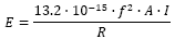
where f is the signal frequency in Hz, A is the loop
area in m2, I is the current amplitude in the loop in Ampere, and
R distance to the loop in meters.
As example, a 1cm2 current loop with 1mA
current with 100MHz frequency at 3m distance generates a field strength of 4.4µV/m
or 12.9dBµV.
Figure 1 below shows the approximate radiation of a
1cm2 current loop with 1mA current at 3m distance as a function of
the frequency of the current. The green line shows the approximate EN55013 radiation
limit for 3m distance.
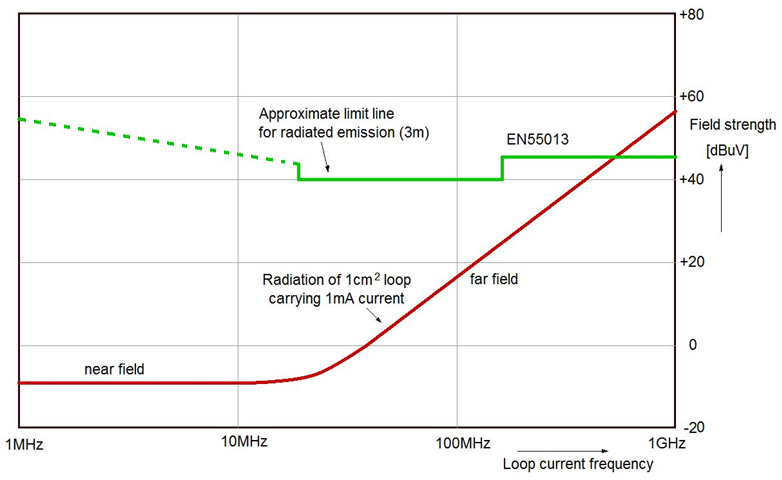
Figure 1
From the figure, it can be seen that radiation of a
1cm2 loop with 1mA rms high frequency current will not easily exceed
limits. The problem that often leads to exceeding the limits is when smaller
loops excite bigger loops or wiring attached to the PCB starts radiating. These
bigger loops or wires are much more effective antennas and will therefore have
much higher contribution to total radiation.
3. Identifying current loops in a Buck converter
The DC/DC buck converter has two main loops where high
AC currents flow as shown in figure 2.
When the high-side MOSFET Q1 is on, the current flows
from supply via Q1 and L1 to the output capacitor and the load. The current
flows back via ground to the input. The AC portion of the current will flow
via the input and output capacitors. This current is shown in red color as I1
in figure 2.
When Q1 switches off, the inductor current will keep
flowing in the same direction, and the synchronous rectifier MOSFET Q2 is switched
on. The current flows via Q2, L1, load and output capacitor and back via ground
to Q2. This loop is shown in blue as I2. Both I1 and I2
are discontinuous currents, meaning that they have sharp rising and falling
edges at the beginning and end of the active time. These sharp edges have fast
rise and fall times (high dI/dt). Therefore they have a lot of high frequency
content.
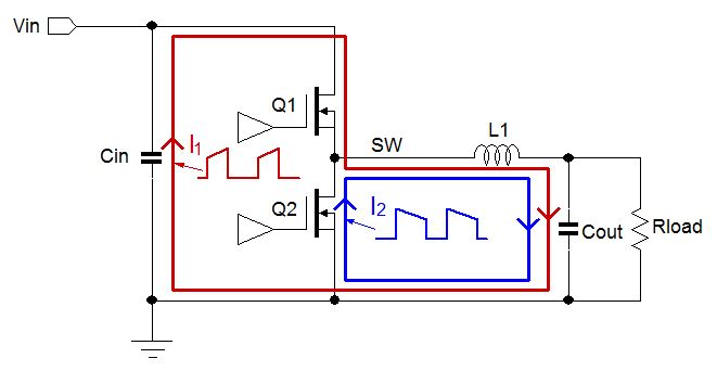
Figure 2 : Buck converter current loops
I1 and I2 share a common path
from switch node to inductor to output capacitor to ground back to the source
of Q2. The sum of I1 and I2 is a relatively smooth continuous
saw-tooth waveform, which has less high frequency content due to the absence
of high dI/dt edges.
From EMI radiation point of view, the current loop with
the high dI/dt current is the shaded area A1 as shown in figure 3.
This loop will generate the most high frequencies and should be considered the
most critical loop for EMI in buck converters. The dI/dt of the current in area
A2 is not nearly as high as in A1 and generally generates
a lot less noise.
Figure 3
When setting up the PCB layout of a buck converter,
shaded area A1 should be made as small as possible.
See
chapter 7 for practical tips on layout.
4. Input and output filtering
In ideal case, the input and output capacitors would
be very low impedance for the buck converter switching currents. But in practice,
capacitors will have ESR and ESL, which increases the capacitor impedance and
results in extra high frequency voltage drop across the capacitor. This voltage
will induce currents in the supply input line and connections to the load, as
shown in figure 4.
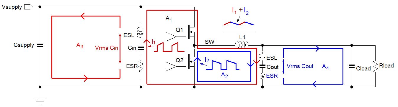
Figure 4
Due to the discontinuous nature of the buck converter
input current and the fact that the supply lines to the converter are often
quite long, the input loop A3 can radiate considerably or result
in exceeding conducted emission levels in the conducted EMC measurements (150kHz
~ 30MHz band)
To reduce the voltage drop across Cin, use low ESR MLCC
types and multiple capacitors of different size like 2x10µF 1206 and one
22n~100nF 0402 or 0603 size type close to the buck IC. To reduce the noise in
the input loop, it is highly recommended to add extra L-C filtering in the input
line. When using pure inductance for L2, it may be necessary to add the electrolytic
capacitor C3 to damp any input supply ringing and ensure stable input supply.
To filter the output, also use multiple different size
MLCC for Cout. Small 0603 or 0402 size 22nF~100nF capacitors can better block
high frequency noise that may be coupled from switch node onto the output via
the parasitic capacitance of the inductor L1. An additional HF bead will avoid
the output loop from becoming an effective loop antenna. It should be noted
that HF beads in the output can deteriorate the load transient response and
load regulation. If the application load is critical in this respect, don’t
use beads but place the converter as close as possible to the load, and minimize
the loop area by using copper planes in the output.
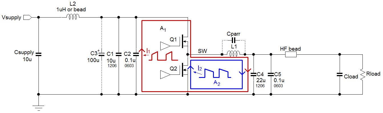
Figure 5 : Buck converter input and output filtering
5. Reducing buck converter switching speed
If the radiation levels of the buck converter circuit
still exceed requirement levels and layout or filtering cannot be improved,
then reduction of the buck converter switching speed can help reducing the radiation
levels. To understand the radiation reduction that can be achieved, let’s
examine the frequency content of a discontinuous current pulse waveform.
Figure 6 left side shows the simplified current waveform
as a trapezoidal wave with period TPERIOD, width TW and
rise and fall times TRISE. The frequency domain will consist of the
fundamental frequency and many upper harmonics. The relation between the pulse
width, rise/fall times and amplitude of the upper harmonics can be derived via
Fourier analysis and is shown in figure 6 right side.
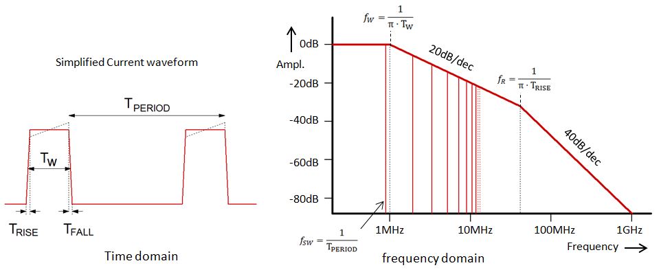
Figure 6 : Harmonic content of a pulse waveform
The figure 6 frequency values are based on an example
with 800kHz switching signal with a pulse width of 320nsec and 10nsec rise and
fall times. Radiated EMI problems often occur in the 50MHz~300MHz range, and
it can be seen that increasing rise and fall times will shift the fR
point to lower frequency, and the high frequencies will roll-off more quickly
with 40dB/dec. In the lower frequency range, the impact of slower rise and fall
times is quite limited.
Adding series resistor in bootstrap circuit.
The switching waveform rise time is determined by the
switch-on speed of the high-side MOSFET Q1. Q1 is driven by a floating driver
that is supplied via a bootstrap capacitor Cboot. In integrated buck ICs, C
boot is charged via an internal regulator (normally 4~5V). See figure 7 left
side.
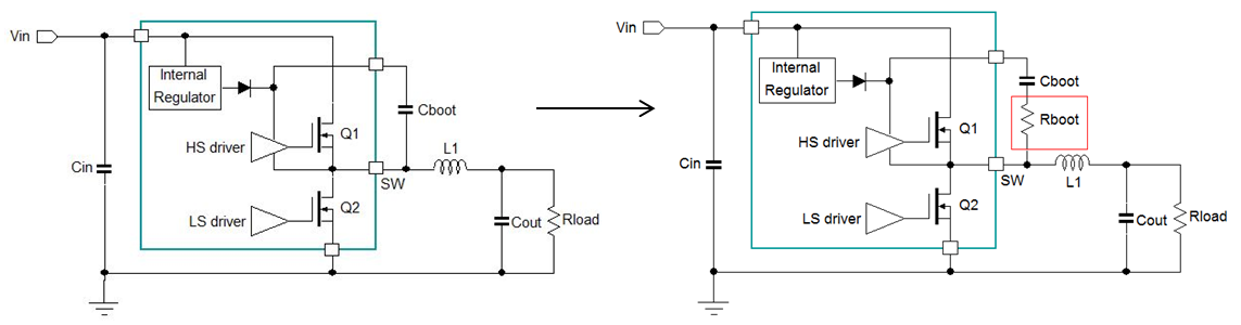
Figure 7 : Adding series resistor in bootstrap circuit
Increasing the rise time of the buck converter switch
waveform and current pulse can be accomplished by slowing down switch-on speed
of the high side MOSFET, which can be accomplished by adding a resistor Rboot
in series with Cboot as shown in figure 7 right side. The value of Rboot depends
on the size of the high side MOSFET. For most applications around 5~10Ω
is used. For smaller (higher Rdson) MOSFETs, larger Rboot values are allowed.
Too high values for Rboot may cause insufficient Cboot charging in high duty-cycle
applications, or cause instabilities in the IC current sense. Slower MOSFET
switch-on will also increase switch losses and reduce efficiency.
In designs were the MOSFETs are external, it is possible
to add a series resistor in high-side MOSFET gate. This will increase the high-side
MOSFET switch-on time and switch-off time.
When the high-side MOSFET Q1 is switched off, the inductor
current will charge the parasitic output capacitance of Q1 and discharge the
parasitic output capacitance of Q2 until the switch waveform goes below ground
and activates the body diode of Q2. The falling time is therefore basically
determined by the inductor peak current and the total parasitic capacitance
at the switch node.
Figure 8 shows an example of the parasitic components
of a buck converter IC in a typical layout.
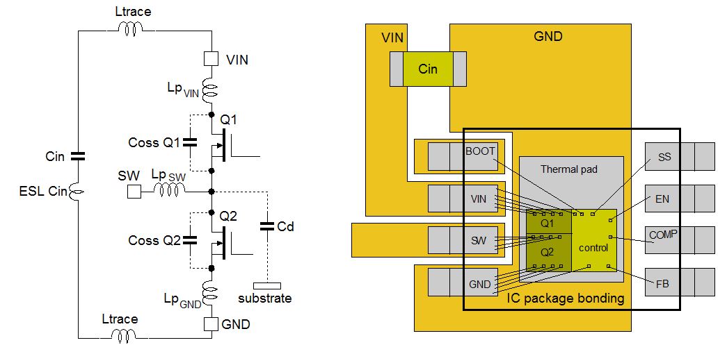
Figure 8
The parasitic capacitances are caused by the MOSFETs
Coss and capacitance to substrate. The bonding wires from IC pins to silicon
die will have some parasitic inductance. These parasitic components in combination
with the PCB layout parasitic inductance and input filter capacitance ESL will
cause high frequency ringing in the switching waveforms. When the MOSFET Q1
switches on, the ringing frequency in the positive edge is mostly determined
by Coss Q2 and the total parasitic inductance in the MOSFET switching loop (LpVIN
+ LpGND + LpLAYOUT + ESLCIN).
When the MOSFET Q1 switches off, the ringing frequency
in the falling edge is mostly determined by Coss Q1 and the parasitic inductance
in the low-side MOSFET source to ground (LpGND).
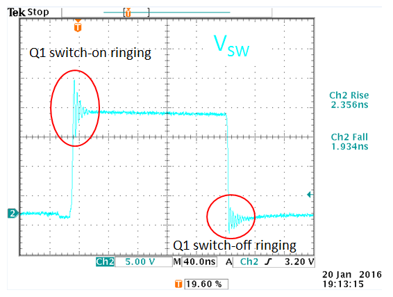
Figure 9
Figure 9 shows an example of a switching waveform with
fast rise and fall times and positive edge and negative edge ringing. Due to
the energy ½∙I2∙Lp stored in the parasitic inductance, the
ringing amplitude will increase with load current. The frequency range will
often be around 200~400MHz and results in high frequency EMI radiation. Excessive
ringing often points to larger circuit parasitic inductance, and the layout
should be checked for bigger loops or thin traces in Vin or ground. Component
package can also influence ringing: bonding wire packages will perform worse
than flip-chip packages due to the higher inductance of bonding wires compared
to pillar bonds.
RC snubber damping
Adding an RC snubber can effectively damp out ringing,
at the expense of increased switching losses.
The RC snubber should be placed as close as possible
to the switch node and power ground. In buck converters with external MOSFETs,
the RC snubber should be placed directly across the drain and source of the
low side MOSFET. Figure 10 shows the placement of the RC snubber.
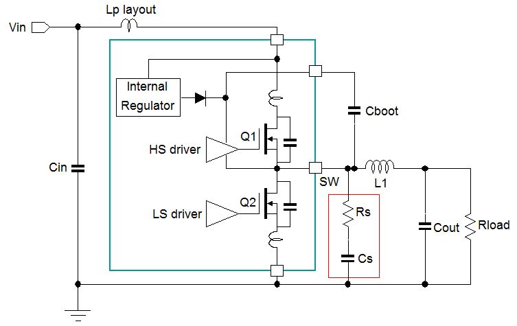
Figure 10
The aim of the snubber resistor Rs is to add sufficient
damping to the parasitic resonant LC circuit. The value for Rs depends on the
desired damping and the parasitic L & C components of the circuit and is
given by :

where ξ is the damping factor. Normally ξ can
range from 0.5 (slightly underdamped) to 1 (critically damped).
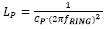
The values for parasitic Lp and Cp are normally not
known, and can best be measured in the following way :
1. Measure the original ringing frequency fRING
in the rising edge.
2. Add some small capacitance from switch node to ground,
and watch the ringing frequency become lower. Keep adding capacitance until
the ringing frequency is 50% of the original ringing frequency.
3. A 50% reduction in ringing frequency means that the
total resonance capacitance is four times the original capacitance. The original
capacitance Cp is therefore 1/3 of the added capacitance.
4. The parasitic inductance Lp can now be calculated
by
The series capacitor Cs of the RC snubber needs to be
large enough that the damping resistor can perform steady resonance damping
during the circuit ringing. Too large values for the capacitor will increase
power loss due to the charging and discharging of the capacitor each switch
cycle. Normally Cs is chosen 3~4 times larger than the circuit parasitic capacitance.
Besides resonance damping, the RC snubber will also
slightly increase rise and fall times of the switching waveform. However, the
charging and discharging of the snubber capacitance will result in extra switching
peak current spikes during switching transitions, which may increase EMI in
lower frequency areas.
After placing the RC snubber, be sure to check the total
power loss of the circuit : The converter efficiency will drop, especially at
high switching frequency and high input voltages.
RL snubber damping
A less obvious way to damp ringing in the switching
circuit is the addition of an RL snubber in series with the resonant circuit.
The buck converter with RL snubber is shown in figure 11. The aim is to add
a small amount of series resistance in the resonant circuit, sufficient to provide
some damping. Due to the fact that the total resistance of the switching circuit
is normally quite low, this damping resistor Rs can be low as well, in the order
of 1Ω or less. The inductor Ls is chosen to provide low impedance at lower
frequencies than the resonance, basically to short-circuit the damping resistor
in the low frequency range. Since the ringing frequency is normally quite high,
the required inductor can be small as well, in the order of a few nH, which
can be achieved via a few mm of thin PCB trace, so it does not significantly
increase the loop area. It is also possible to use a very small bead in parallel
with Rs as substitution for Ls; in that case the bead must have low impedance
at frequencies well below the resonance frequency, and must have sufficient
current rating for the input RMS current.
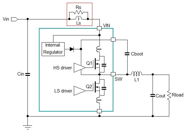
Figure 11
The RL snubber can best be placed close to the power
stage input node. One drawback of the RL snubber is that it creates impedance
Rs in the switching loop the high frequency region. During the very fast switch
transitions, the switch current pulse will create a short voltage glitch across
Rs, resulting in a small voltage glitch on the power stage input node. If this
VIN voltage glitch reaches too high or too low values, the power stage switching
or IC operation may be affected. Be sure to check the voltage glitch on VIN
node during maximum load switching when the RL snubber is added.
6. Practical example
In this chapter shows the effects of several aspects
of buck converter design on EMI. We use RT7297CHZSP, a flexible 800kHz, 3A current
mode buck converter in PSOP-8 package which is tested in a 12V – 3.3V/3A
application. The schematic of the test setup is shown in figure 12.
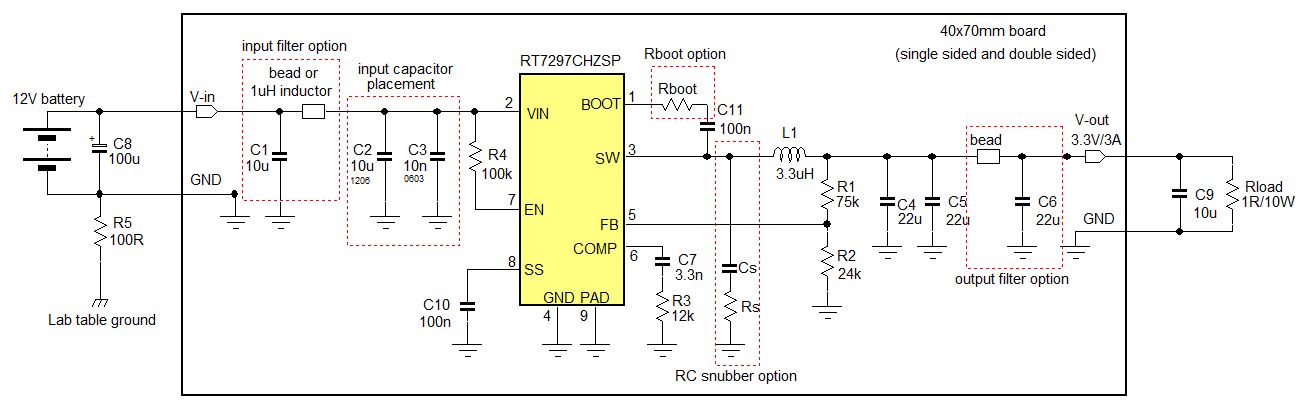
Figure 12
The test board was made in two versions : one with full
copper ground plane and one without ground plane.
The board has several options like LC input filter,
different input capacitor placement, Rboot and RC snubber option and output
LC filter option. The test layout with the different options is shown in figure
13.
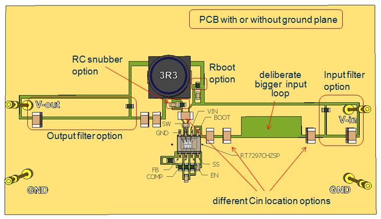
Figure 13 : EMI test board
The test measurement setup is shown in figure 14.
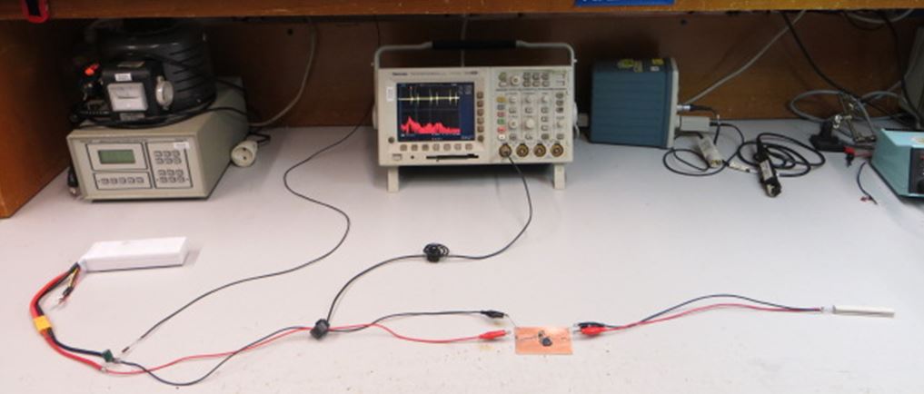
Figure 14
When the board under test is placed on the lab table,
the PCB current loops and wiring will radiate HF energy to the environment.
This radiation finds its way back to the board as high
frequency common mode current in the supply leads. See figure 15. The high frequency
common mode current in the supply leads is basically the combined radiated field
current from the board, and can be used as an indication of radiated emission
when doing experiments.
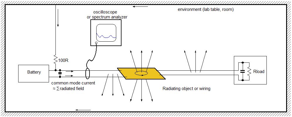
Figure 15 : Common mode current caused by field radiation
The input supply for the converter is provided by a
3S (~12V) Li-Ion battery, to be independent of other lab equipment. There is
an electrolytic capacitor across the battery leads to eliminate resonances due
to battery inductance.
The converter load is a 1Ω resistor in parallel
with a 10µF MLCC capacitor. This provides a 3A load to the converter with
low impedance for high frequencies.
The ground lead of the input line at the battery end
is connected via 100Ω to the lab bench ground. This gives the circuit a ground
reference, with impedance similar as the EMC measurement LISN network.
The self-made EMI current measuring tool (see
chapter 8) can be placed in the supply input and output wires. In this report,
we use an oscilloscope to view the measured HF current signal, which will show
high frequency glitches during the converter switching transitions. For these
repetitive switch signals, it is possible to let the oscilloscope calculate
the FFT of the noise signal, to see the frequency content of the measured current.
Although this is nowhere as accurate as a spectrum analyzer, it is still quite
useful for experiments and judgment on a simple circuit.
Input capacitor placement
Experiment 1 : Place Cin far from the IC
The layout in figure 16 shows a bad placement of the
input capacitor, resulting in a switching loop with lots of parasitic inductance.
(The layout has some extra gap to increase the loop area)
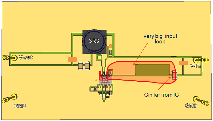
Figure 16
We first do a general check on radiated noise by measuring
the common mode current in the input wires
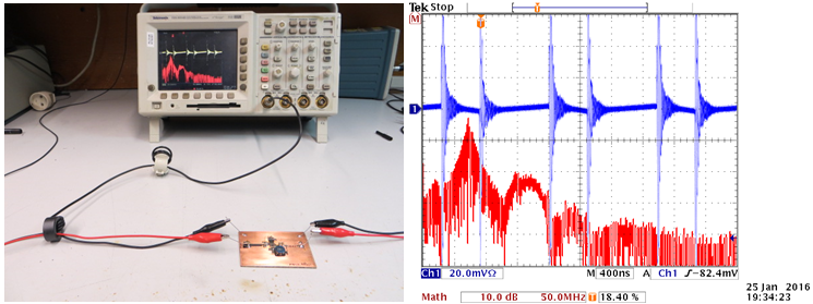
Figure 17 : Common mode current measurement in input wires
Figure 17 right side shows that the common mode current
is extremely high and extends over a wide frequency band.
We can examine the source of the common mode current
by using the loop antenna to search for radiated fields on the PCB. When the
loop antenna tool is held above the input loop, the scope shows a lot of radiated
noise in low and mid frequency range up to 200MHz above the Cin loop, see figure
18.
We also see that the switching waveform has a very big
overshoot and ringing, actually exceeding IC voltage ratings. So the bad placement
of the input capacitor gives both high radiation and big waveform ringing.
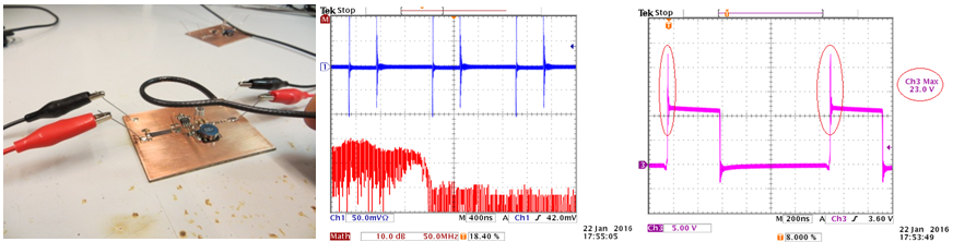
Figure 18 : Measuring radiated field from big CIN
loop on single sided PCB
If we do the same measurement on the board with a ground
plane on bottom side, it can be seen that the radiation from the big Cin loop
with the ground plane is much lower than with the single sided board. Switching
ringing is also slightly lower in the board with the ground plane, see figure
19.
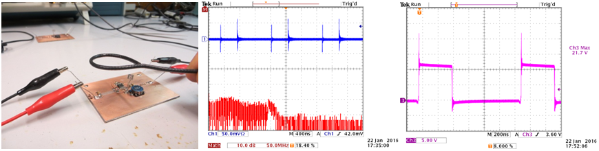
Figure 19 : Big CIN loop on double sided PCB
with ground plane
The HF magnetic field from the big loop creates eddy
currents in the bottom ground plane which create a field in opposite direction
that partly cancels the original magnetic field. The closer the ground plane
to the loop, the more effective it will be.
Experiment 2 : Cin closer to the IC.
We continue with the single sided PCB, and place the
Cin capacitor close to the IC, which results in a much smaller Cin loop. See
figure 20.
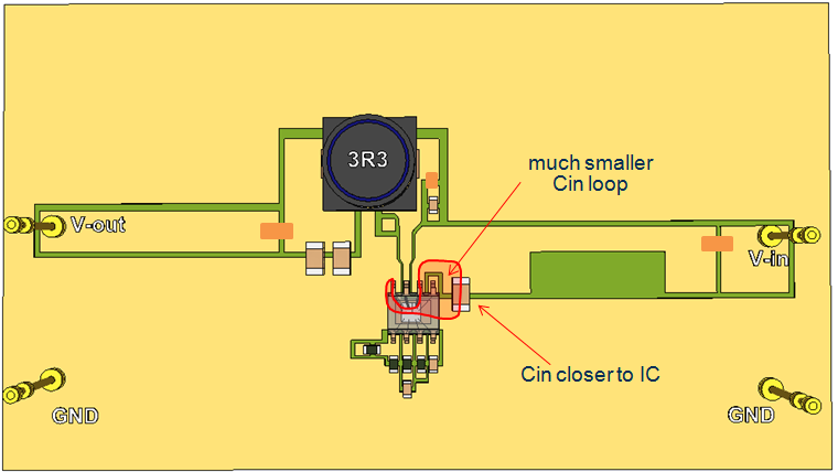
Figure 20 : Better placement of CIN
The switching overshoot and ringing is around 50% lower,
and radiated emission has dropped around 10dB.
The frequency band extends now to 300MHz range.
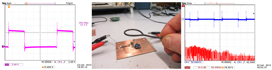
Figure 21
It is important to realize that the better placement of
Cin will improve both switching waveform overshoot & ringing and reduce
the HF radiation.
|
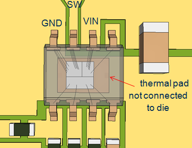
In RT7297CHZSP, the thermal pad is not connected
to the die, so the layout copper connection to the thermal pad does
not shorten the Cin loop. The high side and low side MOSFETs are
connected via multiple bonding wires to the VIN and GND pin. So
the shortest loop is via these two pins.
|
|
Experiment 3 : Add an additional small 10nF capacitor
directly between the IC VIN and GND pins.
Figure 22 shows the placement : The Cin loop is
now basically determined by the IC pins, bonding wires and 0603 capacitor
size.
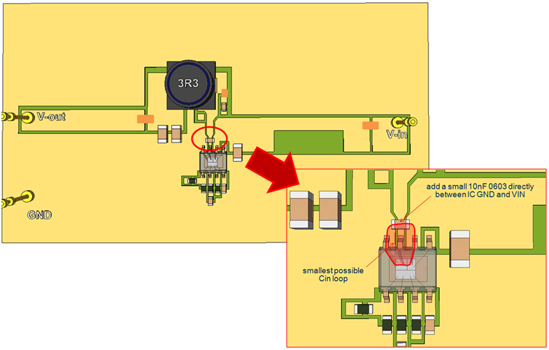
Figure 22
The switching waveform overshoot is virtually gone,
but a lower frequency ringing has appeared.
The measurement loop has to be positioned closer
to the PCB : The high frequency noise is gone, but there is a large peak
in the low frequency area around 25MHz.
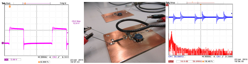
Figure 23 : Adding single 10nF 0603 between ic GND
and VIN pins
The low frequency resonance is a result of two capacitors
in parallel in different loops with different resonances. This often happens
during EMI trouble shooting, and the loops and resonances should be identified.
In this case, the 10nF resonates with a 4nH parasitic inductance (~3mm conductor
length), creating a 25MHz resonance. The resonant loop is the small 0603
capacitor with IC pins, bonding wire and layout traces, which make a loop
with around 3mm length.
The solution can be found by adding a large 1206 22µF
capacitor with slightly higher ESR in parallel to the small 10nF capacitor.
The layout with optimal Cin capacitor locations is
shown in the layout of figure 24.
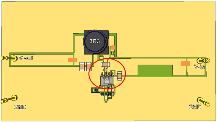
Figure 24
With above solution, the single sided board switch
waveform overshoot is virtually gone, and the radiated noise pick-up from
loop antenna is also very low; the FFT waveform is mainly at the noise floor
level.
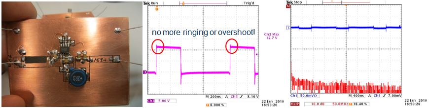
Figure 25 : Final solution with shortest CIN
loop
If we now measure the common mode current in the
input wire with the HF current probe, we see that the common mode noise
has dropped a lot, more than 30dB at some frequencies when compared with
the first measurement. This means that the total board radiation level is
now quite low.
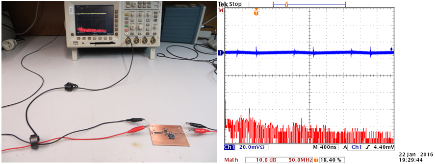
Figure 26 : Final solution common mode measurement
Input supply wire filtering
The high frequency current in the input supply wire
consists of both differential mode and common mode currents. Common mode
noise can be reduced by minimizing the area of the high dI/dt current loops
in the board layout. Input wire differential mode current has different
source. It can be measured with the self-made current probe by passing the
+ and – wires through the core in opposite direction as shown in figure
27 below :
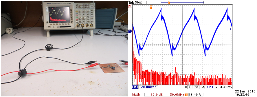
Figure 27 : Differential mode current measurement
The differential current that we measure is caused
by the buck converter pulsing input current passing through the input capacitors,
causing a voltage drop across the capacitance and ESR of the input capacitor
and layout ESL if it is included in the loop. This voltage drop results
in a differential mode a current in the input supply wires.
It is possible to reduce this differential mode
current by increasing the input capacitance, but it is much more effective
to add a small LC filter in the input wire as shown in figure 28 right side.
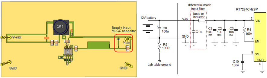
Figure 28 : Input filtering
| Without
extra input filter |
With
input filter 10µF 1206 MLCC + 0603 bead 2A BLM18PG121SN1
|
With
input filter 10µF 1206 MLCC + 1µH inductor LQH3NPN1R0
1.5A |
|
Figure 29
As can be seen from figure 29, adding a bead +
capacitor will remove all high frequency except the 800kHz fundamental;
Using a 1µH inductor + capacitor will remove all differential
mode noise including fundamental.
Output wire filtering
When measuring the differential mode in the output
supply, there is not much high frequency content, due to the continuous
output current without high dI/dt. There is however considerable lower
frequency noise up to around 30MHz. Most of the differential current
in the output leads is caused by the converter inductor ripple current
passing through the output capacitors, which also have some ESR. Adding
an extra LC filter by means of bead and MLCC capacitor as shown in figure
30 will remove most of the differential noise.
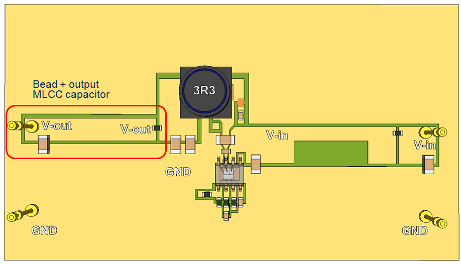
Figure 30 : Output filtering
|
Measuring differential mode current in the 3.3V output leads
|
Without extra output filter |
With output filter 22µF 1206 MLCC + 0603 bead 4A BLM18SG700TN1
|
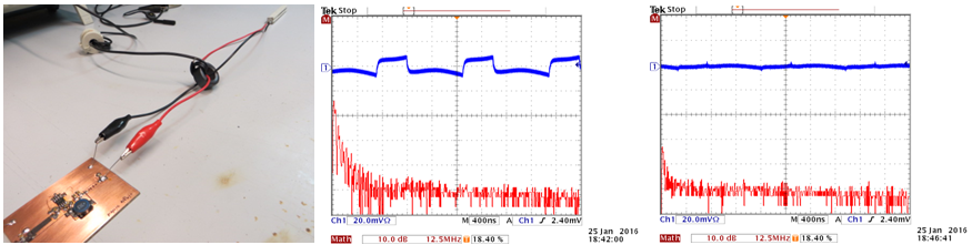
|
Figure 31
Quite often, some inductor stray magnetic field
is coupled into the output loop as well.
Shielded inductor types have low stray fields
and will not easily couple into the output loop. But in case non-shielded
or semi-shielded inductors are used, the output loop area to the
load needs to be minimized to avoid stray magnetic field coupling.
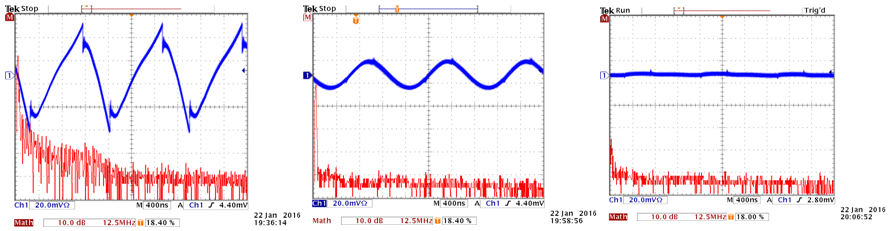
Reducing ringing by adding series resistance
in bootstrap circuit and RC snubber.
For this experiment, we use the double sided
board with input capacitor location as shown in experiment 2. This
setup gives significant radiation from the input loop.
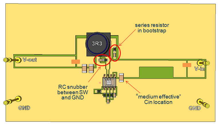
Figure 32
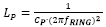
As reference measurement, the input supply
common mode current was measured without Rboot or RC snubber. The
switch waveform shows 5V overshoot with 238MHz ringing frequency.
Common mode current in the supply wires shows considerable high
frequency noise, see figure 33.
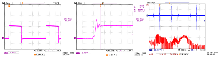
Figure 33 : Reference measurement switch waveform
and common mode current
RT7297C has a relatively small high side
MOSFET (110mΩ), so the impact of adding low values of series
resistance to the bootstrap circuit is relatively small. It was
found that Rboot needed to more than 20Ω to see any change
in the switching waveform. Below scope picture shows the original
waveform with 0Ω (reference in grey) and the new waveform
when adding 33Ω series resistance, reducing the overshoot
to 3V. The impact of this change to the common mode current was
very small, hardly measureable in this simple measurement setup.
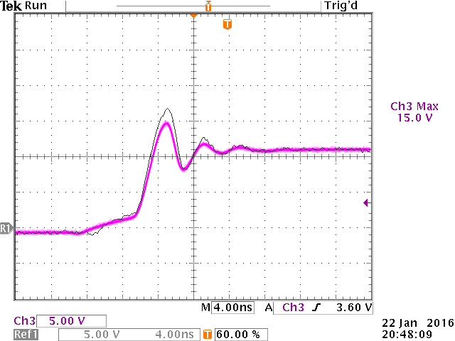
Figure 34 : Ringing before and after adding
33Ω Rboot
For determining the RC snubber values, we
use the method as described in
chapter 5 :
Original fRING = 238MHz. After
adding 220pF, fRING becomes 114MHz. CP is
thus 220pF/3 = 73pF.
LP can be found from
 ; LP = 6.1nH.
RS can be calculated from
 ; when we use ξ = 0.5 we get RS = 9.1Ω, we choose
8.2Ω
; when we use ξ = 0.5 we get RS = 9.1Ω, we choose
8.2Ω
CS is chosen 4xCP
and becomes 330pF.
|
Waveform before RC snubber |
Waveform after RC snubber |
Common mode with snubber |
|
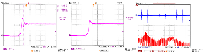
Figure 35 : Effect of RC snubber on
switch waveform and common mode current
Adding the RC snubber will reduce the
common mode current in high frequency range around 5dB.
|
Rising edge is clean without ringing |
Falling edge has not changed much |
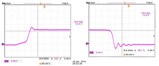
|
Figure 36 : Switching waveform with
both solutions : RC snubber 8.2Ω & 330p and 33Ω
Rboot
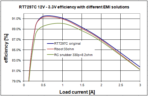
Figure 37 : The difference in efficiency
when snubber and Rboot are added
As can be seen, Rboot has little
effect on efficiency, except a small efficiency drop at
higher load.
The RC snubber has more impact on
efficiency, especially in the low and mid load range, but
still only 1~2% max, which is acceptable. It should be noted
that buck converters that operate at higher switching frequency
and higher input voltages will show higher losses when snubbers
are applied.
7. Buck converter layout tips
A good buck converter layout starts
with good planning where to place the key components.
1. In noise sensitive applications,
choose buck converters in small, low inductance flip-chip
packages.
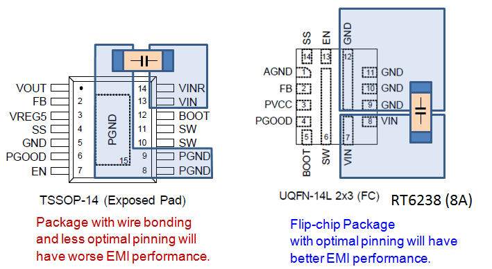
Figure 38 : Different packages will
give different input loop area and stray inductance.
2. Identify the VIN and GND node
of the switching loop, and place different size input capacitors
as close as possible between these nodes, the smallest size
capacitor closest to the nodes. This input switching loop
carries the very high dI/dt currents, and should be kept
as small as possible.
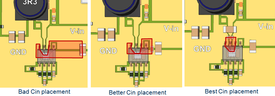
Figure 39 : Layout examples with different
input capacitor placement
3. Place the output capacitor ground
in an area that does not overlap the input capacitor switching
loop : this could generate extra high frequency noise in
the output voltage.
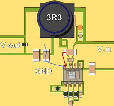
Figure 40
4. The traces from the switching
node and BOOT pin carry high dV/dt voltages, and can cause
some electric field radiation, so the trace copper area
should be kept relatively small, and away from other sensitive
signals.
5. The converter small signal section
should be away from the high power switching section. The
grounding of the small signal section should preferably
be a clean low noise ground point. Do not ground small signal
section in the area where the VIN decoupling currents or
output ripple currents flow, see figure 41 left side.
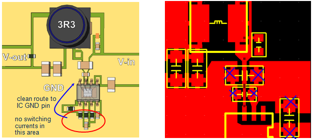
Figure 41
6. Do not use thermal relief in
component layout for critical loops, they create extra inductance
See figure 41 right side.
7. When using ground planes, try
to keep these planes as solid as possible below the input
switching loop. Any trace that cuts the ground plane in
this area will reduce the ground plane effectiveness. Signal
vias create holes in the ground plane, increasing impedance
as well.
8. Vias can be used to connect decoupling
capacitors and IC ground to the ground plane, and loop can
be shortened. But keep in mind that via inductance can range
from 0.1~0.5nH (depending on via thickness and via length),
and may increase the total loop inductance. Multiple vias
should be used for lower impedance connection.
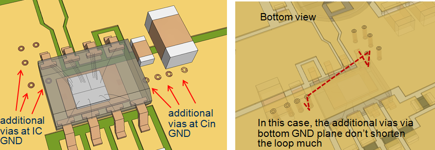
Figure 42
In above example, the additional
vias to bottom ground plane do not help a lot in reducing
the Cin loop. But in other cases where the top layer loop
is long, reducing loop area with vias to the ground plane
is quite effective.
9. Note that using the ground plane
as return for loop currents will make the ground plane noisy.
You can isolate by using a local ground planes, and connect
it to the main ground at a point with lowest noise.
10. Ground planes loop shielding
effectiveness increases when they are closer to the radiating
loop. In multi-layer PCBs, place the solid ground plane
on layer 2, directly below the top layer that carries the
high power currents.
11. Non shielded inductors generate
a lot of magnetic stray fields, which can radiate into other
loops or filter components. Semi-shielded or fully shielded
inductors should be used in noise sensitive applications
and sensitive signals and loops should be kept away from
the inductor.
8. Simple EMI probing tools you can
build yourself
Measuring EMI compliance often means
you have to bring the prototype product to an EMI facility
for testing. These are normally 3m sites in anechoic chambers,
with special measurement setups using antennas and expensive
measurement receivers. The measurement data shows the final
results of the complete setup, but it is not always easy
to find the root cause of specific radiation frequency emissions
from these 3m measurements.
It is possible to do some basic
EMI measurements on a prototype product in the lab environment,
and examine system blocks separately. These measurements
are normally near-field (measuring distance < 0.16λ),
so for measuring radiation that originates from current
loops, you need a small loop antenna for measuring high
frequency magnetic fields. A small electrically shielded
loop antenna can be easily made yourself using a length
of thin 50Ω coaxial cable : see figure 43.
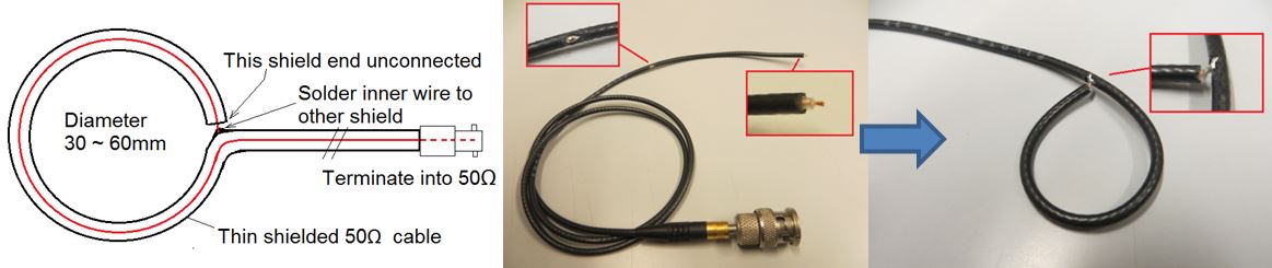
Figure 43 : Loop antenna construction
The loop antenna can be connected
to a spectrum analyzer and by moving the loop over the PCB
of your application, you can see which areas emit a lot
of high frequency magnetic field. You can also connect the
loop antenna to an oscilloscope (terminated in 50Ω)
and the oscilloscope will show switching noise levels in
certain areas of the PCB. By keeping the loop at a fixed
distance and place, and making some changes to circuits/PCB
loops, you can check whether radiated noise levels will
increase or reduce.
Since radiation from supply wires
can contribute considerably to EMI levels, you can also
measure the high frequency current in wiring. Not all current
probes have sufficient bandwidth to highlight EMI, but a
couple of windings on an EMI ferrite core will form a high
frequency current transformer. Construction is similar to
the loop tool, but now the loop has 3 turns around the ferrite
core. See figure 44.
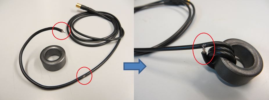
Figure 44 : High frequency current
probe construction
The high frequency current in cables
can now be measured by passing a cable through the ferrite
core. The current transformer output can be connected to
spectrum analyzer or oscilloscope (terminated in 50Ω).
To avoid common mode current flowing
from the tested device to the measurement equipment, it
is recommended to add a common mode choke in the cable :
this can be done by placing a clip-on EMI core with a couple
of windings in the cable to the analyzer.
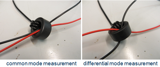
Figure 45
Passing both positive and negative
supply wire in the same direction though the core will measure
the common mode current in the supply wires. Reversing one
wire direction will measure differential mode current, see
figure 45.
Another handy tool is the current
sniffer probe. It is a miniature current transformer with
open core, see figure 46. It can be used to measure high
frequency currents in copper traces or component pins.
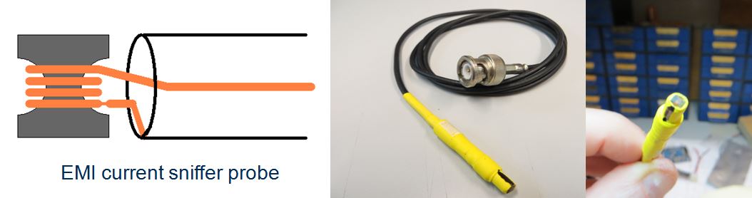
Figure 46 : Current sniffer probe
construction
It is a bit harder to build yourself.
You can grind the open core from a small two holed ferrite
bead and add around 4~5 windings, then connect the windings
to a coaxial cable. It is best to place the core in the
shield opening. When using this tool, you should be aware
that it can pick up some electric fields as well. To determine
whether the measurement result is magnetic field or electric
field pick-up, you can turn the tool 90 degrees on the trace.
Magnetic field measurement will almost reduce to zero, electric
field pick-up will hardly change.
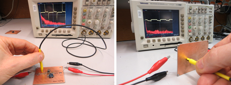
Figure 47 : Current sniffer probe
use
The current sniffer probe will let
you check how various high frequency currents are flowing
through the board and component leads. It can even show
how the currents flow through copper planes : You’ll
find that a high frequency current in a copper plane will
choose the shortest route. Also the eddy currents in the
ground plane can be measured.
All measurements in this document
were made with the tools described here.
9. Conclusion
Solving EMI can be complex, especially
in complete systems without knowing the source of the radiation.
With some basic knowledge of critical high frequency signals
and loops in switching converters, component and layout
behavior at higher frequency and using some simple self-made
tools, it is possible to trouble shoot EMI, pin-point the
radiation sources and find low cost solutions to reduce
radiation.
The major radiation source in buck
converters is the converter input switching loop, and this
loop should be the first focus point. Switching converters
with different package construction can play a role in finding
the best component placement for lowest EMI radiation.
Reducing converter switching speed
can help reduce EMI, but this should not be the first action
to reduce EMI. Shielding by means of ground planes can be
effective, as long as the ground planes are solid and as
close as possible to the radiating loop. Filtering of input
and output supply leads can help to reduce conducted EMI
levels.
References :
Fundamentals of Electromagnetic Compatibility 2nd
edition, by B. Danker