General Description
This document provides information on the function and use of the RTQ6059 evaluation board (EVB), as well as instructions for operating and modifying the board and circuit to meet individual requirements. Additionally, it includes details on the schematic diagram, bill of materials, and evaluation board layout.
Performance Specification Summary
Summary of the RTQ6059GJ8 Evaluation Board performance specificiaiton is provided in Table 1. The ambient temperature is 25°C.
Table 1. RTQ6059GJ8 Evaluation Board Performance Specification Summary
|
Specification
|
Test Conditions
|
Min
|
Typ
|
Max
|
Unit
|
|
Default Input Voltage
|
Default = 12V
|
0
|
--
|
32
|
V
|
|
Supply Voltage
|
Default = 3.3V
|
3
|
--
|
5.5
|
V
|
|
Sensing Current
|
|
--
|
0.5
|
--
|
A
|
|
1 LSB Step Size
|
Sense voltage
|
--
|
10
|
--
|
μV
|
|
Bus voltage
|
--
|
4
|
--
|
mV
|
|
Quiescent Current
|
TA = 25°C
|
--
|
0.7
|
1
|
mA
|
|
Shutdown mode
|
--
|
6
|
15
|
μA
|
Power-up Procedure
Suggestion Required Equipments
- DC Power Supply (Chroma, 62006P-100-25)
- Electronic load capable of 6A
- Richtek Wrenboard
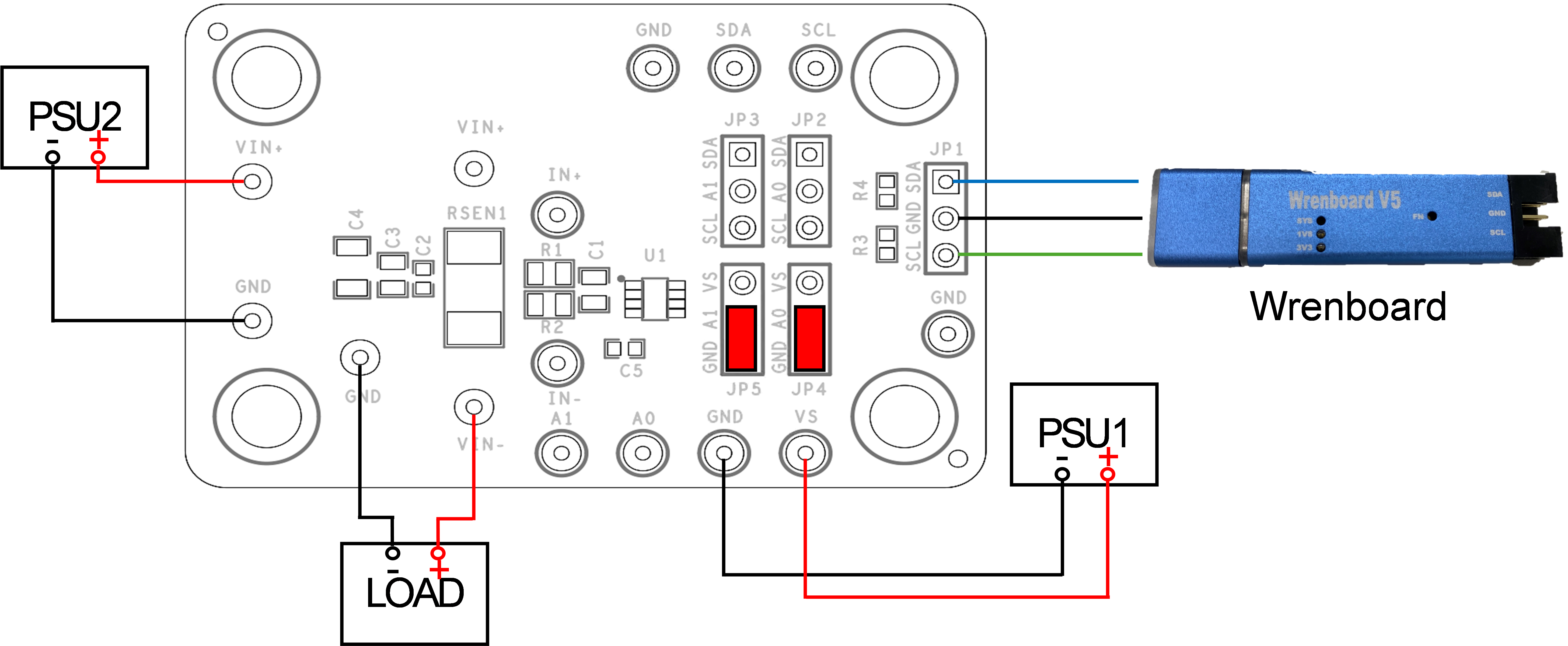
Figure1. High-Side Configuration
Quick Start Procedures
1. Apply VS = 3.3V input power supply (3V < VS < 5.5V) to VS and GND terminals.
2. Apply 12V input power voltage (0V < IN+ < 32V) to the IN+ and GND terminals.
3. The default sense resistance is 100mΩ.
4. Connect an external load to the IN- and GND terminals, and keep loading current = 0.5A.
5. Measure the sense voltage (approximately 50mV) between the IN+ and IN-.
6. Use the RTQ6059 GUI to check practical sense voltage, bus voltage, current, and power.
Detailed Description of Hardware
Headers Description and Placement
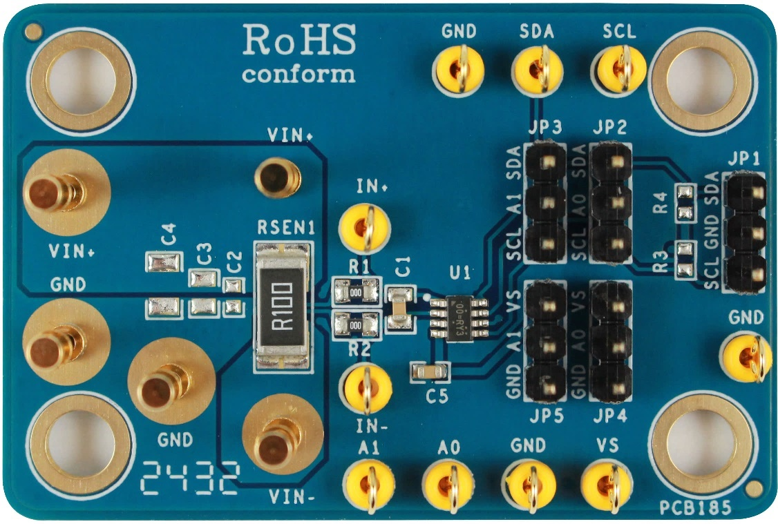
Carefully inspect all the components used in the EVB according to the following Bill of Materials table, and then make sure all the components are undamaged and correctly installed. If there is any missing or damaged component, which may occur during transportation, please contact our distributors or e-mail us at evb_service@richtek.com.
Test Points
The EVB is provided with the test points and pin names listed in the table below.
|
Test Point/
Pin Name
|
Function
|
|
A1, A0
|
Slave address selection.
|
|
SCL
|
I2C communication connection.
|
|
SDA
|
I2C communication connection.
|
|
IN+
|
Positive current-sensing input.
|
|
IN-
|
Negative current-sensing input.
|
|
VS
|
Power supply, 3V to 5.5V.
|
RTQ6059 Evaluation Board Jumper Default Settings
Figure 2 displays the default jumper settings of the RTQ6059 Evaluation Board. The initial slave address, as indicated in Table 2, is 0x40 (Hex). To modify the slave address, the position of the jumper can be altered.
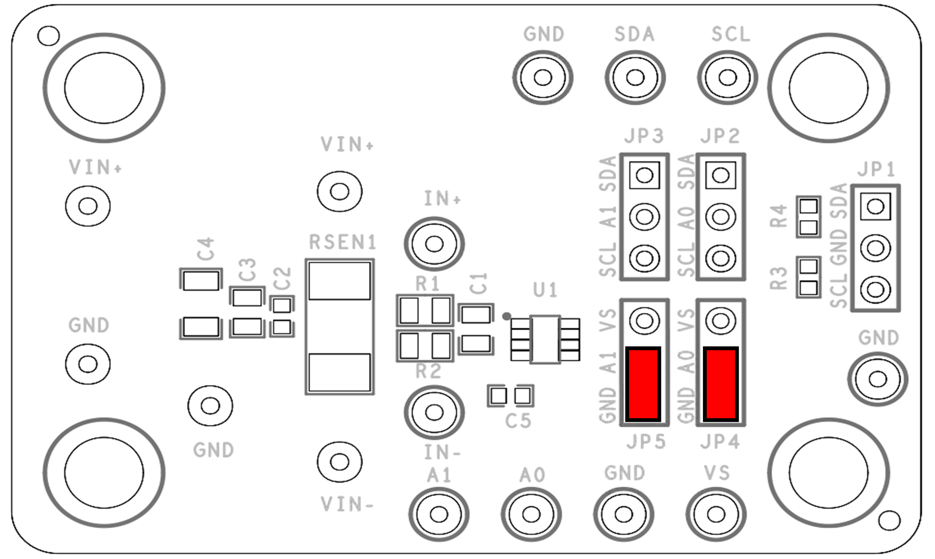
Figure 2. Slave Address Default Setting
Table 2. Slave Addresses Selection
|
A1
|
A0
|
Slave Address
|
Slave Address (Hex)
|
|
GND
|
GND
|
1000000
|
40
|
|
GND
|
VS
|
1000001
|
41
|
|
GND
|
SDA
|
1000010
|
42
|
|
GND
|
SCL
|
1000011
|
43
|
|
VS
|
GND
|
1000100
|
44
|
|
VS
|
VS
|
1000101
|
45
|
|
VS
|
SDA
|
1000110
|
46
|
|
VS
|
SCL
|
1000111
|
47
|
|
SDA
|
GND
|
1001000
|
48
|
|
SDA
|
VS
|
1001001
|
49
|
|
SDA
|
SDA
|
1001010
|
4A
|
|
SDA
|
SCL
|
1001011
|
4B
|
|
SCL
|
GND
|
1001100
|
4C
|
|
SCL
|
VS
|
1001101
|
4D
|
|
SCL
|
SDA
|
1001110
|
4E
|
|
SCL
|
SCL
|
1001111
|
4F
|
IN+ and IN- Input RC Filter
The RTQ6059 Evaluation Board features an RC filter option to shield the IN+ and IN- inputs from high-frequency noise. As depicted in Figure 3, the default settings are 0Ω for resistance and 0.1µF for capacitance.
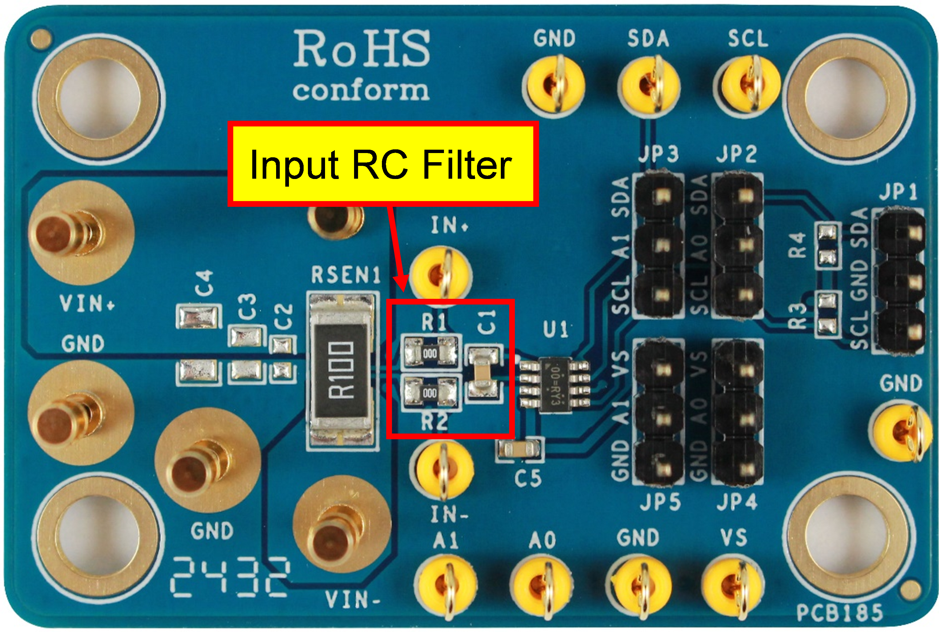
Figure 3. Input Filter Setting
Freely Choose between High-Side or Low-Side
Figure 1 shows the RTQ6059 Evaluation Board in a high-side configuration. To switch to a low-side configuration, as per Figure 4, short the VIN- pin to GND, connect VIN+ to Load +, connect Load - to PSU2 +, and short PSU2 to GND. According to the design architecture, Low-Side Configuration is only suitable for current measurement. This configuration method involves connecting the measurement device between the load and the ground, allowing for the direct measurement of the current passing through the load.
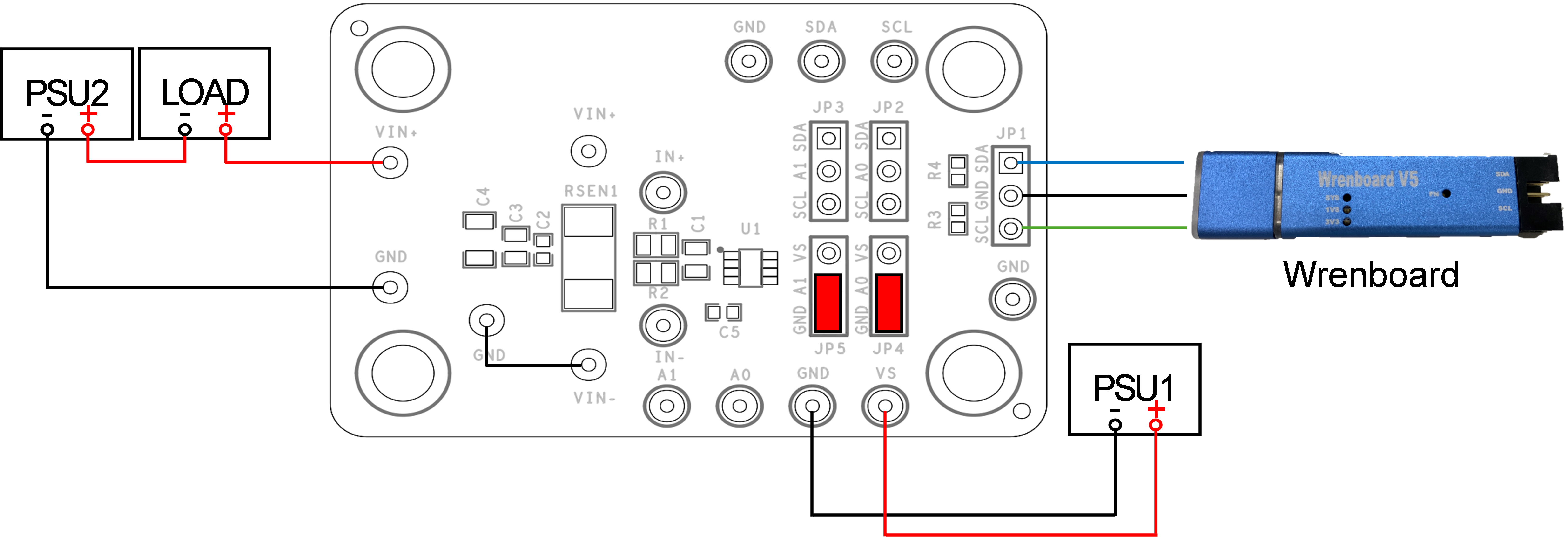
Figure 4. Low-Side Configuration
RichTek WrenBoard Driver Installation
To use the WrenBoard developed by Richtek, it is necessary to first install the driver. Follow the steps below to complete the driver installation, and then the WrenBoard will be ready for use. As shown in Figure 5, click on "Richtek Bridgeboard Utilities" and then press the "Install" button to begin the installation.
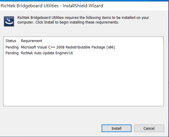
Figure 5. Driver Installation Step 1
As seen in Figure 6, wait for the installation to proceed. During the installation process, a window will pop up, as shown in Figure 7. At this point, press the "YES" button to continue with the installation.
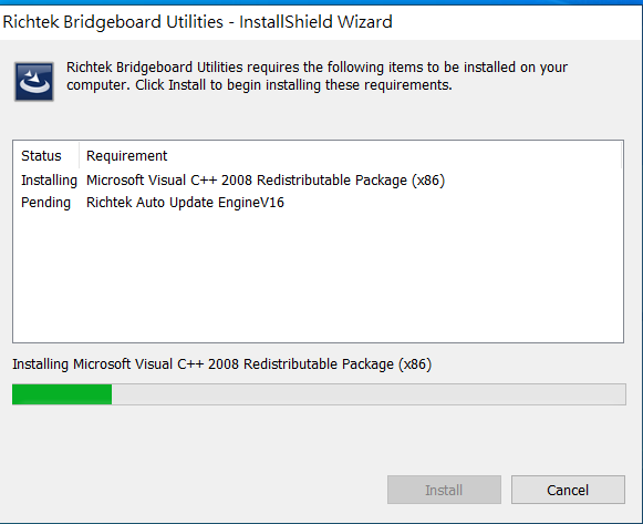
Figure 6. Driver Installation Step 2
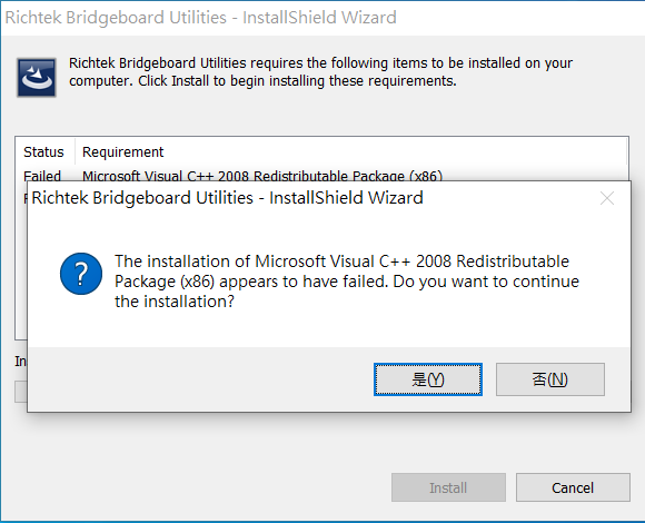
Figure 7. Driver Installation Step 3
The installation will continue at this point. Wait for the installation process to proceed further, as shown in Figure 8.
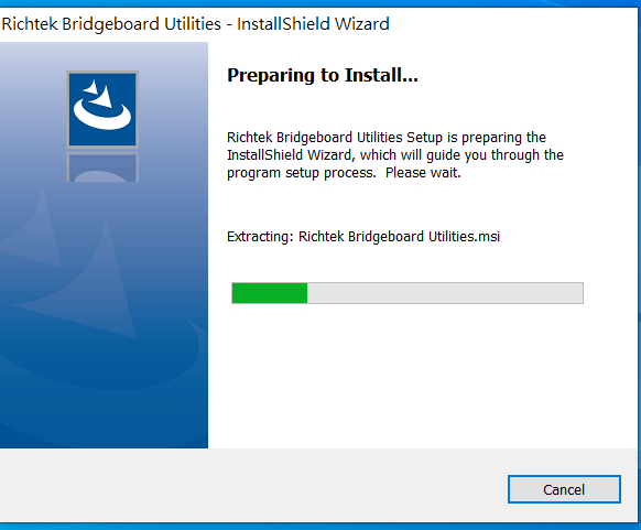
Figure 8. Driver Installation Step 4
After clicking the "Next" button in Figure 9, the License Agreement screen, as shown in Figure 10, will appear. Choose to accept and continue by clicking the "Next" button. Then, after confirming the relevant information in Figure 11, you can click the "Next" button again.
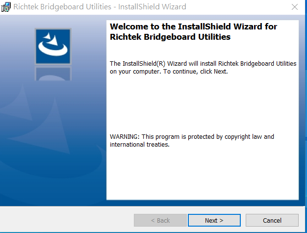
Figure 9. Driver Installation Step 5
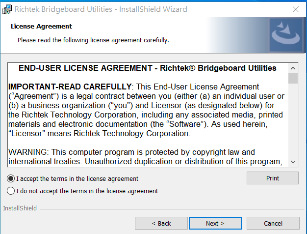
Figure 10. Driver Installation Step 6
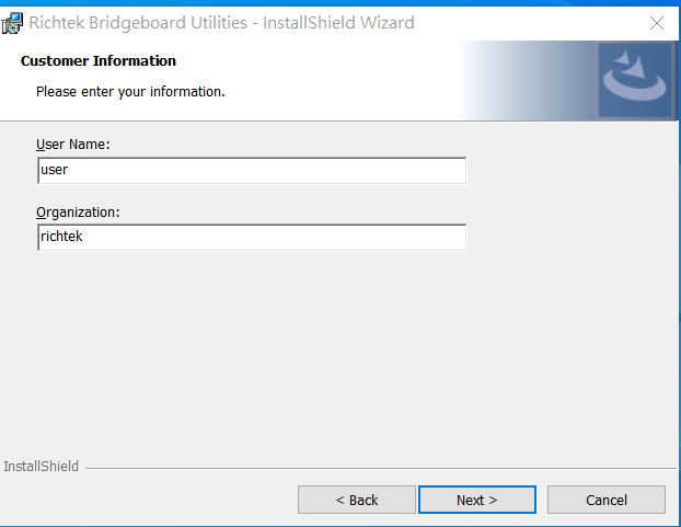
Figure 11. Driver Installation Step 7
In Figure 12, you can set the path for the installation. Once you have set it, you can click the "OK" button. Figure 13 is a confirmation step to ensure the installation path is correct. If everything is satisfactory, you can click the "Next" button to proceed with the rest of the installation.
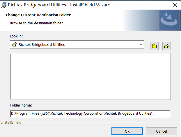
Figure 12. Driver Installation Step 8
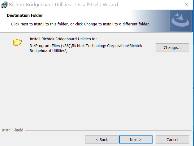
Figure 13. Driver Installation Step 9
As shown in Figure 14, after confirming that all information is correct, click the "Install" button and wait for the installation progress bar to complete, as depicted in Figure 15. Once the installation is fully completed, click "Finish" to complete the entire driver installation process, as shown in Figure 16.
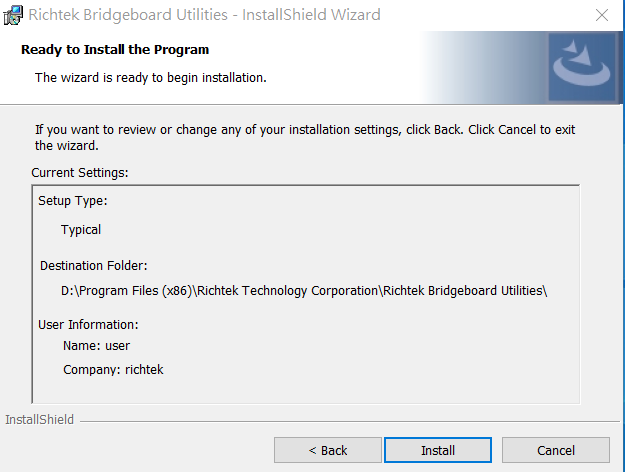
Figure 14. Driver Installation Step 10
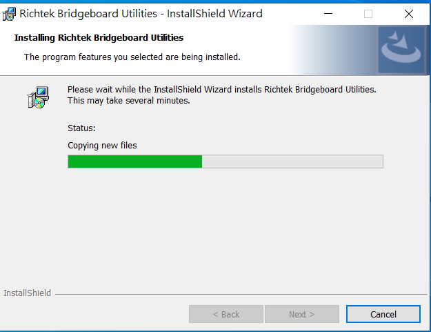
Figure 15. Driver Installation Step 11
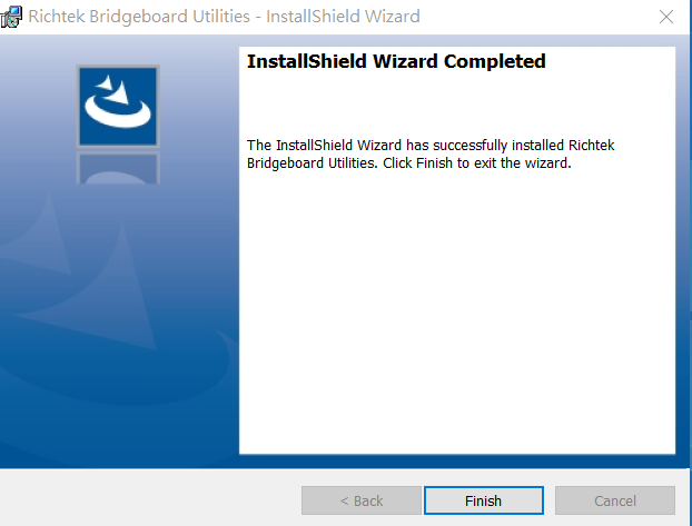
Figure 16. Driver Installation Step 12
RTQ6059 Evaluation Board Software Setup
The GUI for the RTQ6059 can be downloaded from the official website. After downloading, please unzip the file and click the installer to proceed with the installation. Figure 17 demonstrates the installation process.
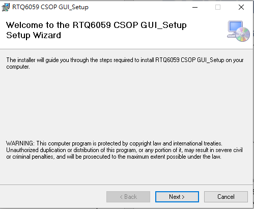
Figure 17. GUI Installation Step 1
During the installation process, set the installation path according to the user’s needs, and then continue with the installation until the software is completely installed, after which the GUI can be used. Figure 18 shows the progress bar of the installation process.
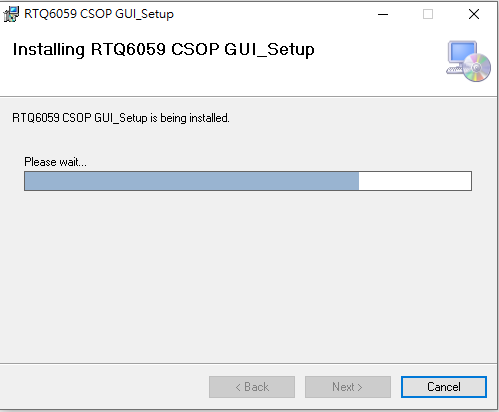
Figure 18. GUI Installation Step 2
Graphical User Interface Overview
The RTQ6059 Evaluation Board includes the RTQ6059 CSOP GUI, which allows users to control the RTQ6059. Figure 19 displays the GUI interface, which is user-friendly.
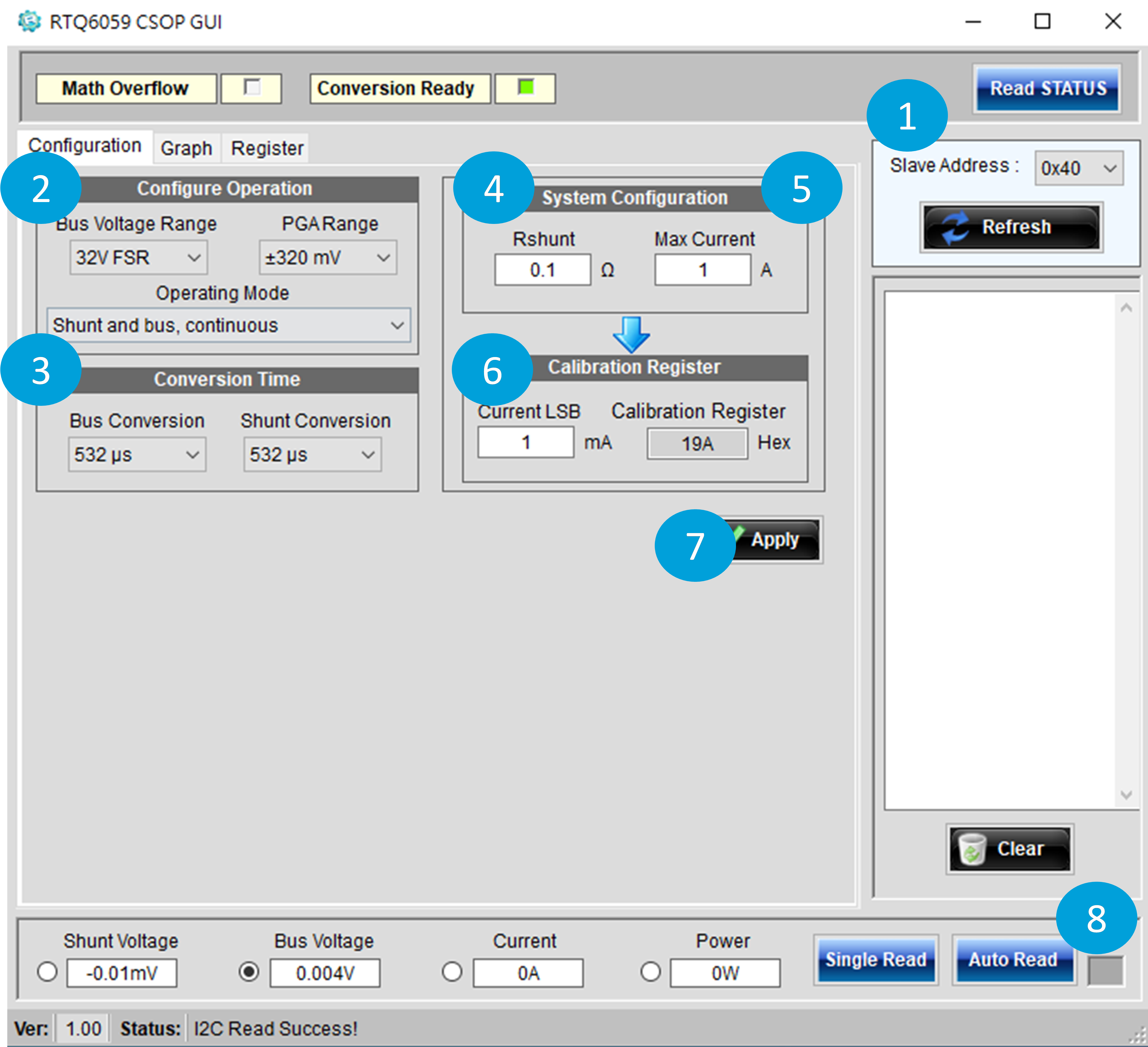
Figure 19. RTQ6059 Graphical User Interface
Quick Operation of the RTQ6059 EVB Software
Step 1. Check Slave Address.
Step 2. Set Configure Operation Mode.
Step 3. Set Conversion Time.
Step 4. Set the shunt resistor value.
Step 5. Set Max expected current for sensing.
Step 6. Set min current resolution for current LSB.
Step 7. Push “Apply” bottom, the 0x05 Calibration register is written into a value for expected current LSB.
Step 8. The data of single read or continued read selection.
Selection of Slave Address
Slave Address is follow Figure 20. Users can connect multiple EVBs and upon clicking the "Refresh" button, the GUI will detect all connected slave addresses.
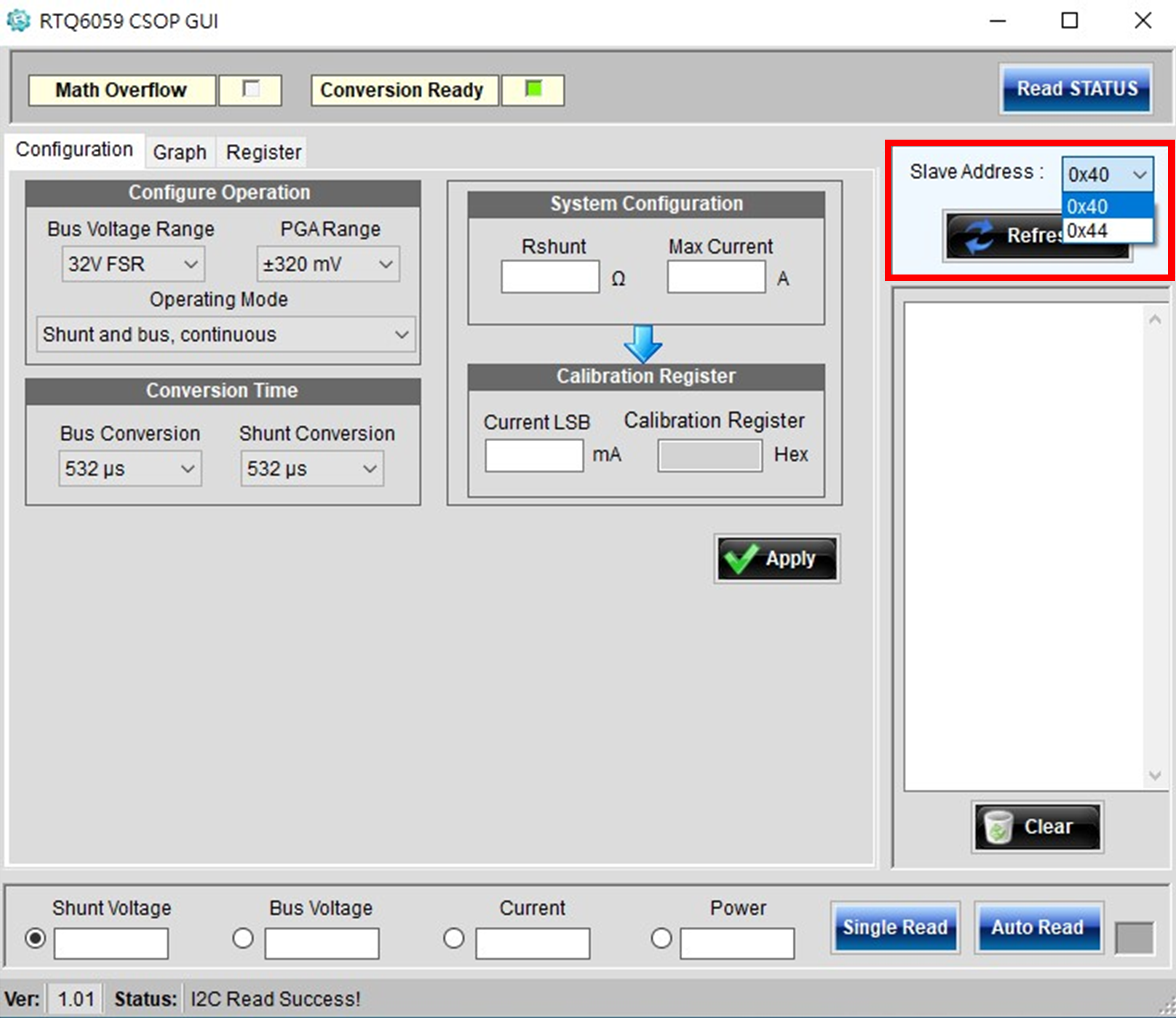
Figure 20. Select Slave Address
Customize the Configuration Operation
This GUI provides configuration options for operations such as setting the Bus Voltage Range, PGA Range, and Operating Mode, as illustrated in Figure 21. Users can decide on all the modes to be set based on their own needs.
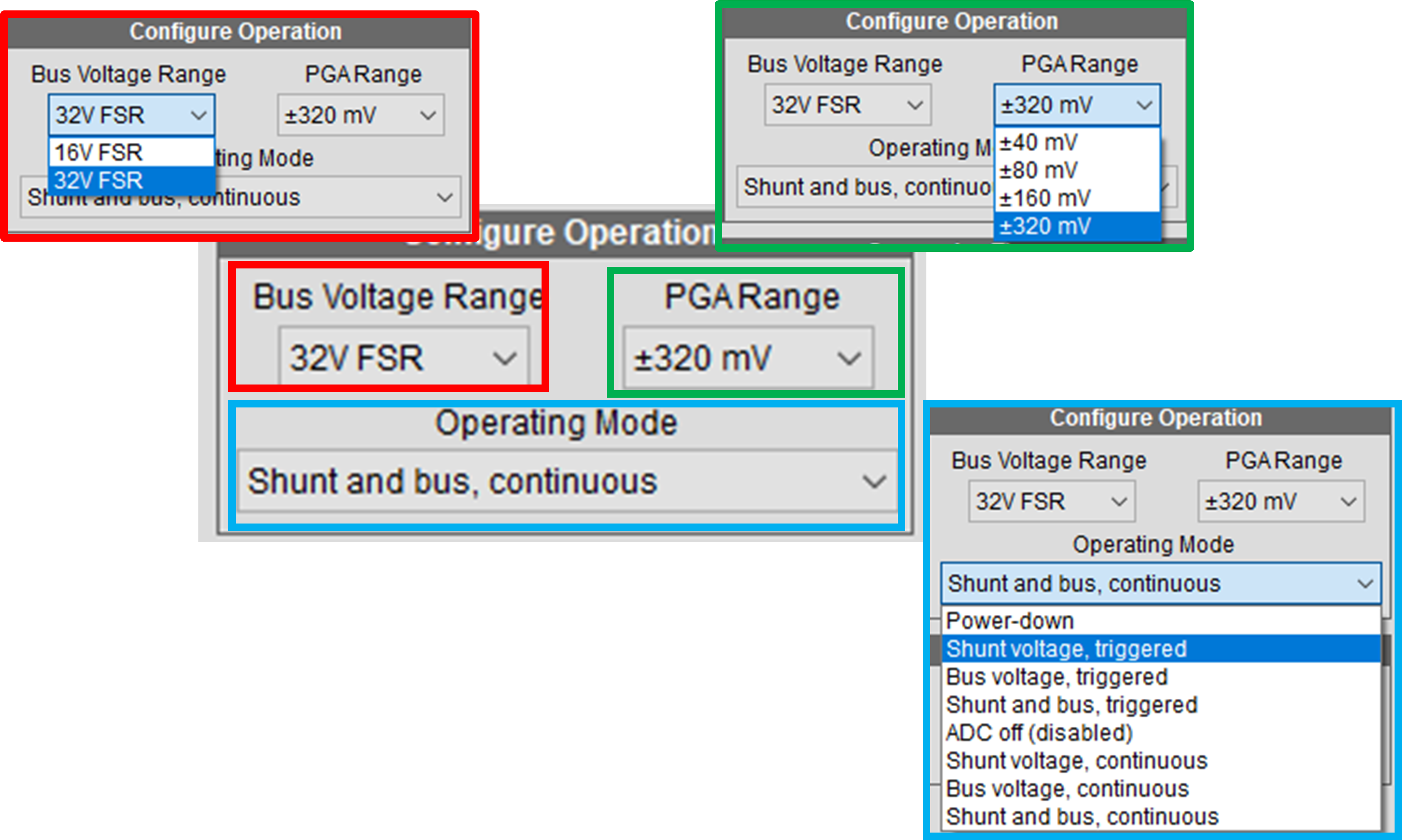
Figure21. Configure Operation
Conversion Time Settings
Users can customize the required conversion times as shown in Figure 22. Both Bus and Shunt settings are configured independently. To observe differences, selecting longer conversion times is advisable.

Figure22. Bus/Shunt Conversion Time Settings
Auto Calibration Function
Users need to correctly configure the compensation values in the Configuration Register to ensure accurate readings are displayed in the software. Setting the correct compensation values requires the following Equation 1, which can be cumbersome for users. Therefore, the GUI provides an automatic compensation calculation method. As shown in Figure 23, by entering the resistance value used, the maximum current, and the minimum current LSB, the final required compensation value can be calculated.
 ……………………………….(1)
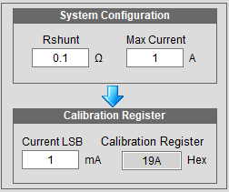
Figure 23. Auto Calibration
Function for Drawing Chart
Figure 24 displays the process when the "Auto Read" button is pressed, depicting the wait for the GUI to capture data. Figure 25 shows that users can select the desired ranges to plot and check them, with the results being immediately displayed on the Graph.
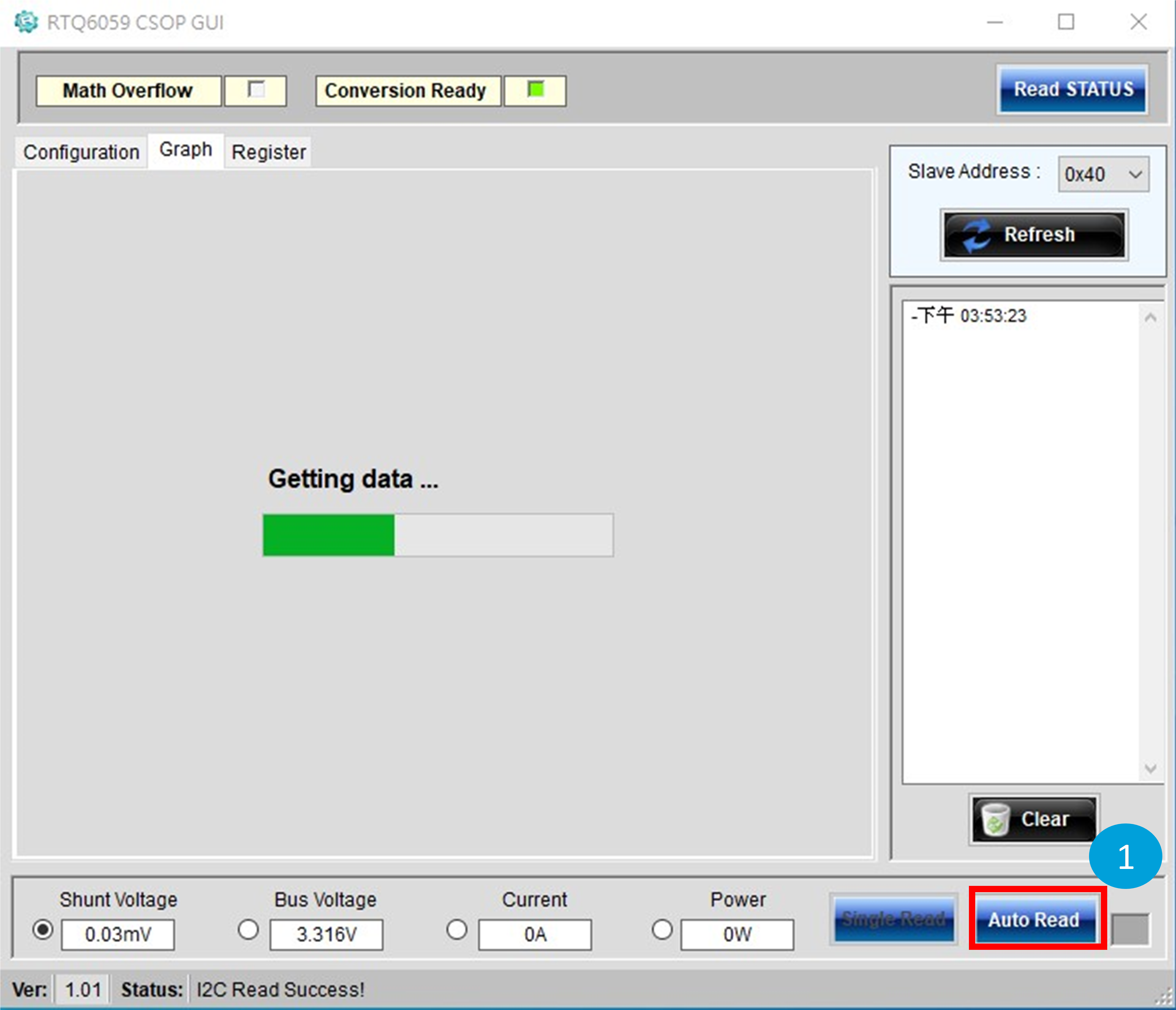
Figure 24. Data Visualization Function
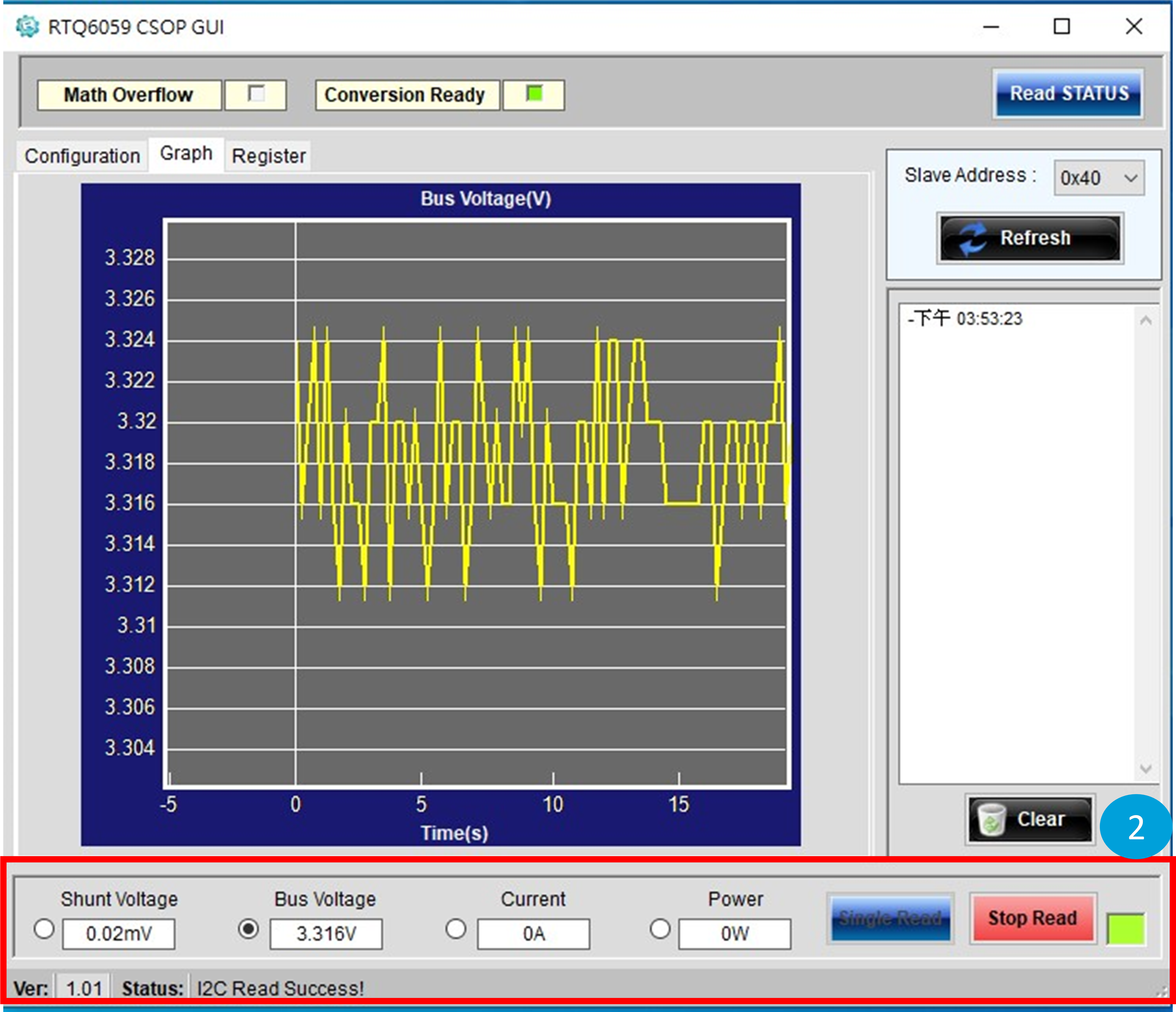
Figure 25. Customize Chart Display Function
Single Register Read/Write
Figure 26 demonstrates the capability to read and write to individual registers through the GUI.
Step 1. Select the register to Read/Write.
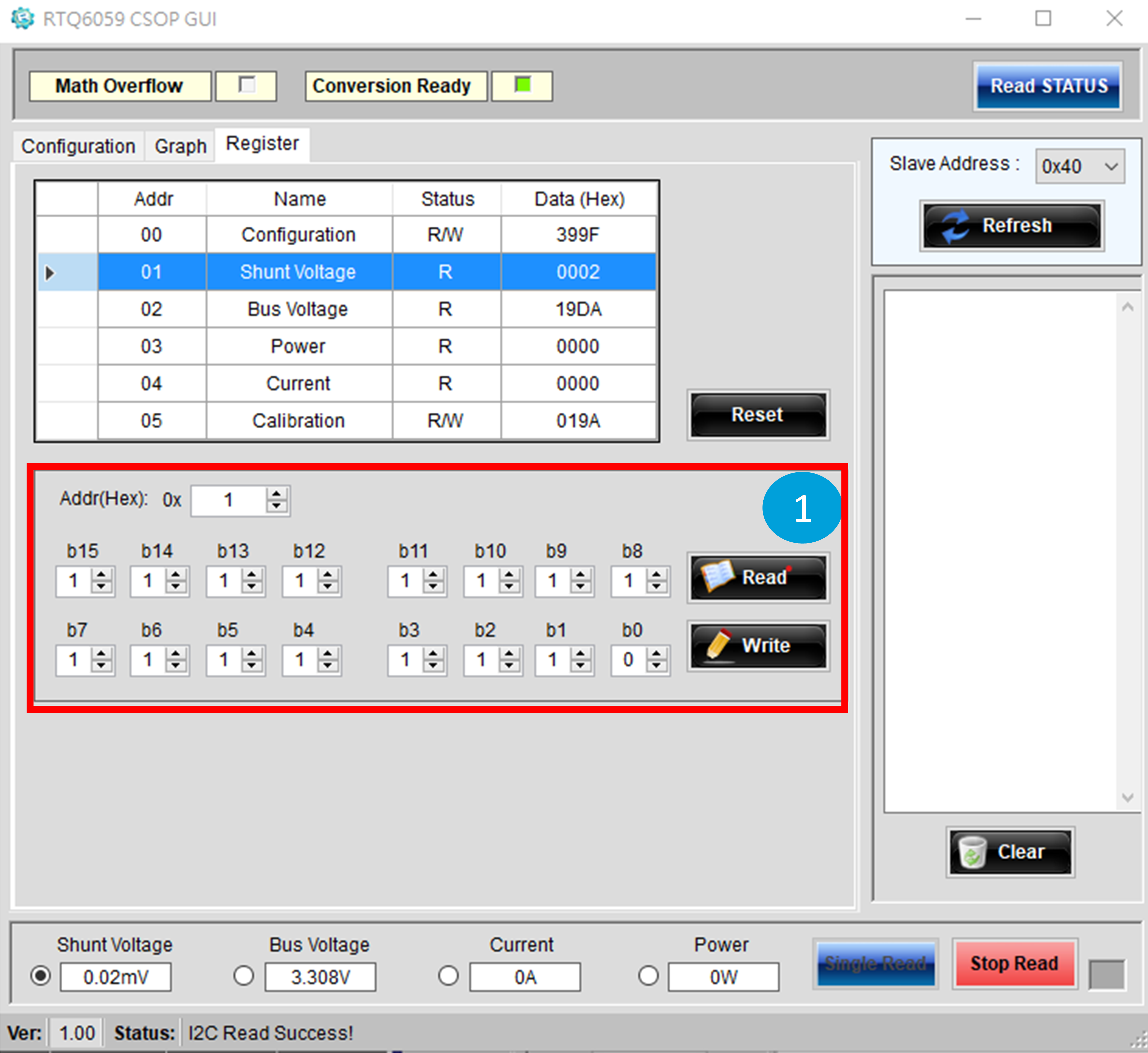
Figure 26. Register Read/Write Function
Bill of Materials
|
VIN = 12V, VS = 3.3V, IOUT = 0.5A
|
|
Reference
|
Count
|
Part Number
|
Value
|
Description
|
Package
|
Manufacturer
|
|
U1
|
1
|
RTQ6059GJ8
|
--
|
16-Bit ADC Op Amp
|
TSOT-23-8
|
RICHTEK
|
|
C1, C5
|
2
|
GRM188R71H104KA93D
|
0.1µF
|
Capacitor, Ceramic, 50V/X7R
|
0603
|
MURATA
|
|
R1, R2
|
2
|
RAT030000FTP
|
0
|
Resistor
|
0603
|
RALEC
|
|
RSEN1
|
1
|
RTT25R100FTE
|
0.1
|
Resistor
|
2512
|
RALEC
|
Typical Applications
EVB Schematic Diagram
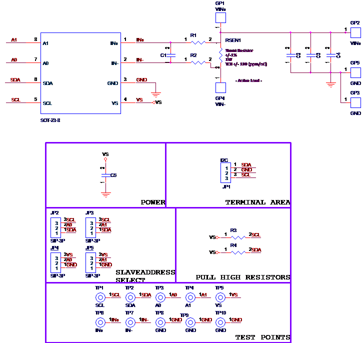
1. The capacitance values of the input and output capacitors will influence the input and output voltage ripple.
2. MLCC capacitors have degrading capacitance at DC bias voltage, and especially smaller size MLCC capacitors will have much lower capacitance.
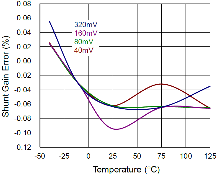
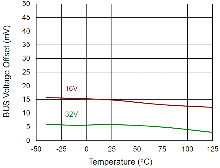
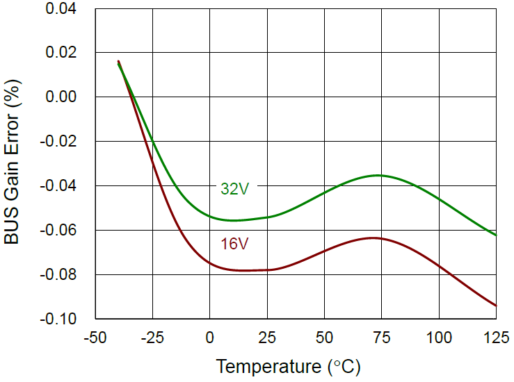
Measurement Results
|
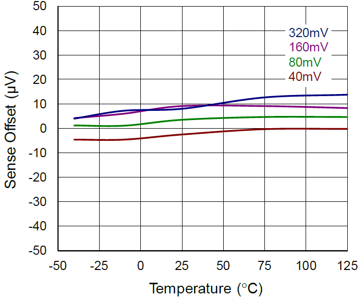
Sense Offset vs. Temperature
|
Shunt Gain Error vs. Temperature
|
|
|
|
|
Bus Voltage Offset vs. Temperature
|
Bus Gain Error vs. Temperature
|
|
|
|
Evaluation Board Layout
Figure 27 and Figure 28 are RTQ6059GJ8 Evaluation Board layout. This board size is 50mm x 33.5mm and is constructed on two-layer PCB, outer layers with 2 oz. Cu and inner layers with 1 oz. Cu.
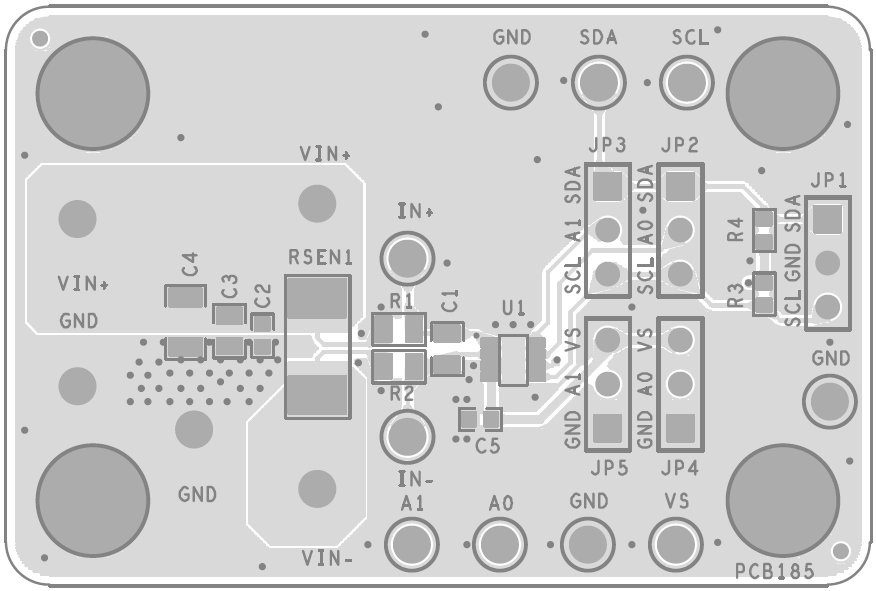
Figure 27. Top View
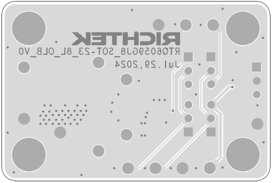
Figure 28. Bottom View