Purpose
The RT8092 is a Peak-Current Mode Pulse-Width-Modulated (PWM) step-down DC/DC converter with I2C control interface. The input voltage range from 2.5V to 5.5V and provides 4A output current. This document explains the function and use of the RT8092 evaluation board (EVB), and provides information to enable operation, modification of the evaluation board and circuit to suit individual requirements.
Introduction
General Product Information
The RT8092 is a Peak-Current Mode Pulse-Width-Modulated (PWM) step-down DC/DC converter with I2C control interface. Capable of delivering 4A continuing output current over a wide input voltage range from 2.5V to 5.5V, the RT8092 is ideally suited for portable electronic devices that are powered from 1-cell Li-ion battery or from other power sources within the range such as cellular phones, PDAs and handy-terminals.
Internal synchronous rectifier with low RDS(ON) dramatically reduces conduction loss at PWM mode. No external Schottky barrier diode is required in practical application. The RT8092 enters low-dropout mode when normal PWM cannot provide regulated output voltage by continuously turning on the upper P-MOSFET. The RT8092 enters shutdown mode and consumes less than 5μA when the EN pin is pulled low. The switching ripple is easily smoothedout by small package filtering elements due to a fixed operation frequency of 3MHz. Along with its small WL-CSP-15B 1.2x2 (BSC) package, it is suitable for applications requiring small PCB area. To increase battery life time, the RT8092 provides low power mode with IQ < 15µA in standby and light-load applications. The RT8092 also includes Dynamic Voltage Scaling (DVS) for system low power applications.
The I2C interface let the RT8092 controllable flexibly to select VOUT voltage level, peak current limit level, PWM control mode, and so on. Other features include soft-start, auto discharge, lower internal reference voltage, overtemperature, and over-current protection.
Product Feature
- 2.5V to 5.5V Input Range
- Low Operation Quiescent Current
►
Normal Mode IQ < 60µA
►
Low Power Mode IQ < 15μA
- Output range From 0.3V to 5.5V
►
Bank 0 : 0.3V to 0.7V
►
Bank 1 : 0.6V to 1.4V
►
Bank 2 : 1.2V to 2.8V
►
Bank 3 : 2.4V to 5.5V
►
The Default Value is 2.8V (VSEL = High) and 1V (VSEL = Low)
- 4A Continuing Output Current
- Support DVS in the Same Bank
►
VOUT Adjusting Range (max, min) is Settable
- High Efficiency
►
90% at 5V→2.8V with 1.5A Load
- 3MHz Fixed-Frequency PWM Operation
►
Auto-PSM/PWM or Force-PWM Selectable
- Support Remote Ground Sensing for Accurate Output Voltage
Key Performance Summary Table
|
Key Features
|
Evaluation Board Number : PCB016_V1
|
|
Default Input Voltage
|
3.3V
|
|
Max Output Current
|
4A
|
|
Default Output Voltage
|
1.0V with VSEL = L
|
|
Default Marking & Package Type
|
RT8092URWSC, WL-CSP-15B 1.2x2 (BSC)
|
|
Operation Frequency
|
Steady 3MHz at all loads
|
Bench Test Setup Conditions
Please carefully inspect the EVB IC and external components, comparing them to the following Bill of Materials, to ensure that all components are installed and undamaged. If any components are missing or damaged during transportation, please contact the distributor or send e-mail to evb_service@richtek.com.
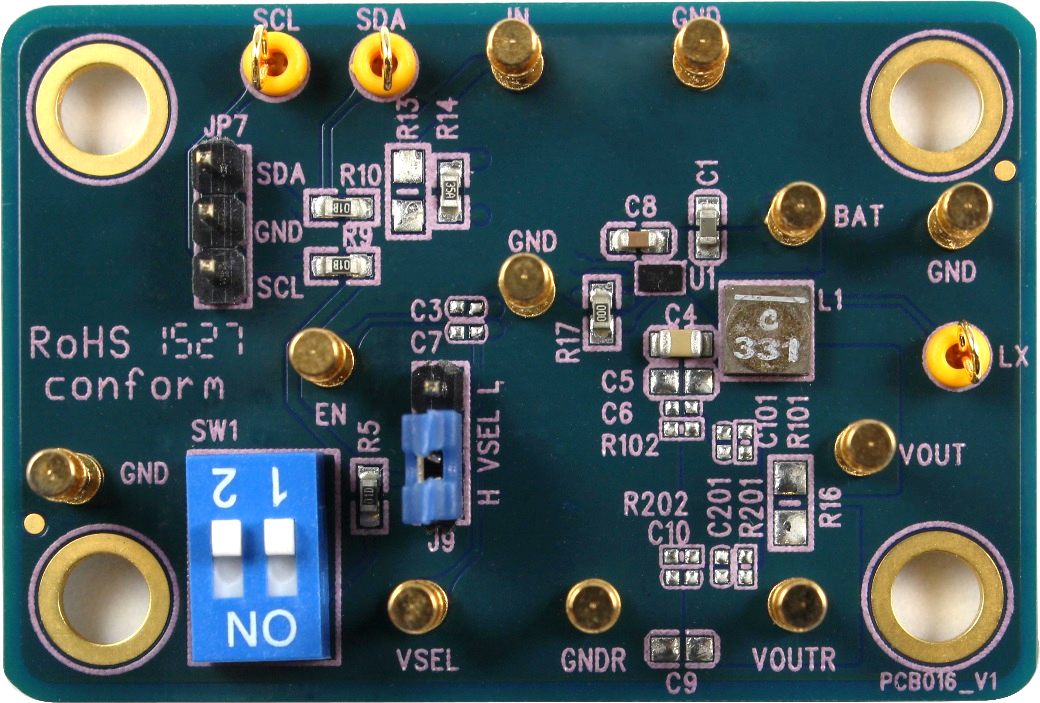
Test Points
The EVB is provided with the test points and pin names listed in the table below.
|
Test point/
Pin name
|
Signal
|
Comment (expected waveforms or voltage levels on test points)
|
|
BAT
|
Input voltage
|
Power input. Support 2.5V to 5.5V Input Voltage. Must bypass with a suitable large ceramic capacitor at this pin.
|
|
EN
|
Enable test point
|
High = Enable.
|
|
GND
|
Ground
|
Ground.
|
|
VSEL
|
Nominal VOUT setting select input pin
|
VSEL = Low selects {0x11.ENSEL0, 0x11.VoutSEL0[6:0], 0x14.PWM0}.
VSEL = High selects {0x10.ENSEL1, 0x10.VoutSEL1[6:0], 0x14.PWM1}.
|
|
VOUT
|
Output voltage
|
Power output. Must bypass with a suitable large ceramic capacitor at this pin.
|
|
VOUTR
|
Output Voltage Sense Input
|
Output feedback pin.
|
|
GNDR
|
Remote Ground Sense Input
|
Connect to GND as short as possible.
|
|
LX
|
Switch node test point
|
Connect this pin to an external L-C filter.
|
Power-up & Measurement Procedure
1. Connect input power (2.5V < VIN < 5.5V) and input ground to VIN and GND test pins respectively.
2. Connect positive end and negative terminals of load to VOUT and GND test pins respectively.
3. There is a 2-pin switch “EN” for enable control. To switch up position to tie EN test pin to input power VBAT for enabling the device. Inversely, to switch down position to tie EN test pin and ground GND for disabling the device.
4. Verify the output voltage (1.0V with VSEL = L or 2.8V with VSEL = H) between VOUT and GND.
5. Connect an external load up to 4A to the VOUT and GND terminals and verify the output voltage and current.
Output Voltage Setting
Set the output voltage by VSEL pin between BAT and GND. There is a 3-pin header “VSEL” for VOUT selection. To use a jumper at “H” option to tie VSEL test pin to input power BAT for VOUT = 2.8V (dafult setting). Inversely, to use a jumper at “L” option to tie VSEL test pin to ground GND for VOUT = 1.0V (default setting).
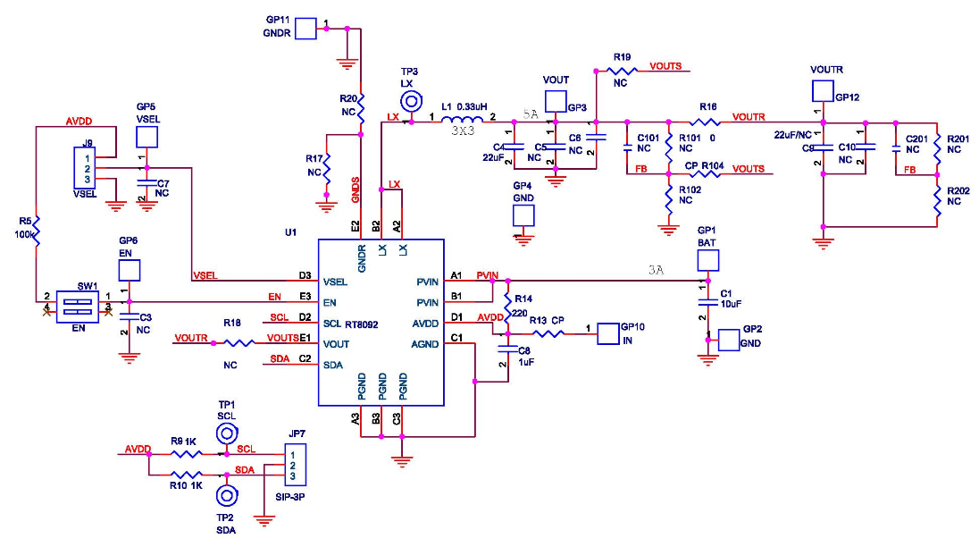
Schematic, Bill of Materials & Board Layout
EVB Schematic Diagram
Bill of Materials
|
Reference
|
Qty
|
Part Number
|
Description
|
Package
|
Manufacture
|
|
U1
|
1
|
RT8092URWSC
|
Buck Converter
|
WL-CSP-15B 1.2x2 (BSC)
|
RICHTEK
|
|
C1
|
1
|
0603X106M6R3
|
10µF/6.3V/X5R
|
C-0603
|
WALSIN
|
|
C4
|
1
|
C2012X5R0J226K
|
22µF/6.3V/X5R
|
C-0805
|
TDK
|
|
C8
|
1
|
C1608X5R0J1A104K
|
1µF/6.3V/X5R
|
C-0603
|
TDK
|
|
R5
|
1
|
RM06FTN1005
|
100k/1%/0603
|
R-0603
|
WALSIN
|
|
R14
|
1
|
RM06FTN2202
|
220/1%/0603
|
R-0603
|
TA-I
|
|
R9, R10
|
2
|
RM06FTN1003
|
1k/1%/0603
|
R-0603
|
WALSIN
|
|
L1
|
1
|
XFL4015-331MEC
|
0.33µH/R33C
|
L-4015
|
Coilcraft
|
PCB Layout
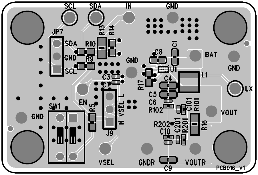
Top View (1st layer)

PCB Layout—Inner Side (2nd Layer)
PCB Layout—Inner Side (3rd Layer)
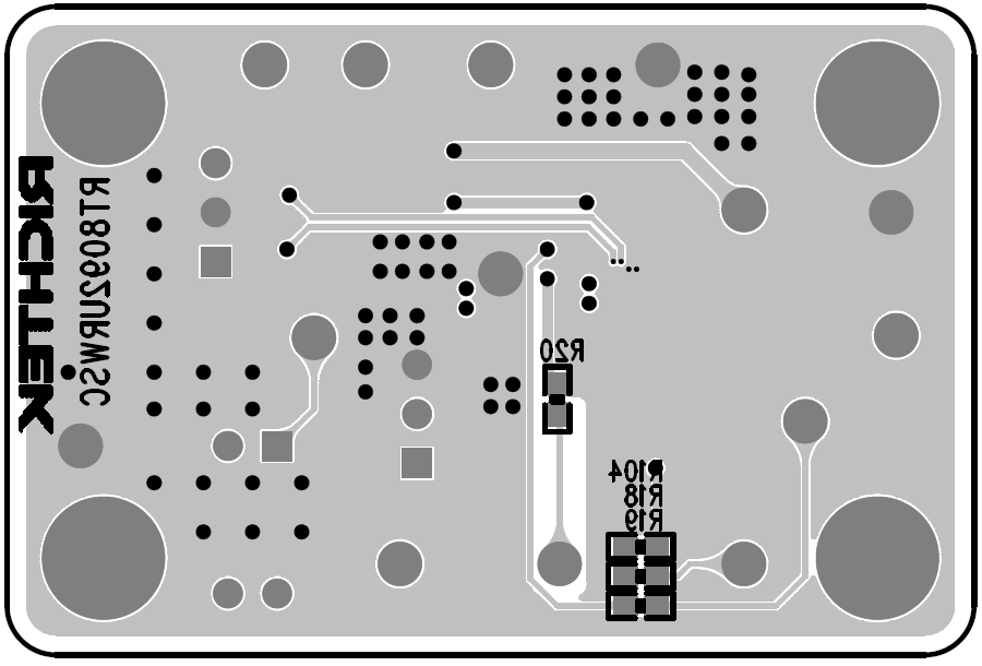
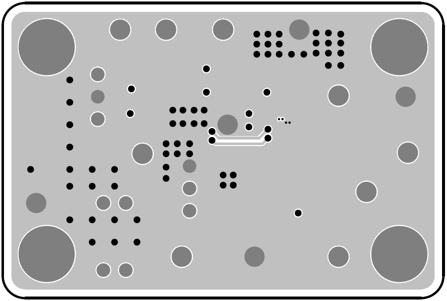
Bottom View (4th Layer)