General Description
The Evaluation Board demonstrates the RT4527A to be designed for high efficiency driver for white LEDs. It is suitable for single/two cell battery input to drive LED light bars which contains six strings in parallel and up to 10 WLEDs per string.
The RT4527A contains I2C interface for controlling the dimming mode, operating frequency and the LED current. The internal 250mΩ, 36V power switch with current-mode control provides overcurrent protection. The switching frequency of the RT4527A is also adjustable from 100kHz to 1.6MHz, which allows flexibility between efficiency and component size.
The RT4527A is available in the WQFN-20L 3.5x3.5 package.
Performance Sepcification Summary
Summary of the RT4527AGQW Evaluation Board performance specificiaiton is provided in Table 1. The ambient temperature is 25°C.
Table 1. RT4527A Evaluation Board Performance Specification Summary
|
Specification
|
Test Conditions
|
Min
|
Typ
|
Max
|
Unit
|
|
Input Voltage Range
|
|
2.7
|
--
|
24
|
V
|
|
Minimum CHx Regulation Voltage
|
|
0.4
|
--
|
0.56
|
V
|
|
LED Channel Current
|
|
6
|
--
|
25
|
mA
|
|
Output Voltage Limit
|
Register address = ‘02h’, 5 bits step = 1V,
default = 36V, COUT = 4.7µF
|
--
|
36
|
--
|
V
|
|
Boost Operates at PWM Mode
|
|
0.1
|
--
|
1.6
|
MHz
|
|
LED Current Accuracy
|
PWM duty = 100%, ICHx = 20mA,
PWM Freq = 1kHz
|
-3
|
--
|
3
|
%
|
|
LED Current Matching
|
PWM duty = 100%, ICHx = 20mA,
PWM Freq = 1kHz
|
-2
|
--
|
2
|
%
|
|
DC Dimming Resolution
|
PWM Freq < 2kHz
|
--
|
4096
|
--
|
Steps
|
|
PWM Freq = 2 to 4kHz
|
--
|
2048
|
--
|
|
PWM Freq = 4 to 8kHz
|
--
|
1024
|
--
|
|
PWM Freq = 8 to 25kHz
|
--
|
512
|
--
|
Power-up Procedure
Suggestion Required Equipments
- RT4527A Evaluation Board
- DC power supply capable of at least 30V and 5A
- LED Load Board
- Function Generator
- Oscilloscope
Quick Start Procedures
The Evaluation Board is fully assembled and tested. Follow the steps below to verify board operation. Do not turn on supplies until all connections are made. When measuring the output voltage ripple, care must be taken to avoid a long ground lead on the oscilloscope probe. Measure the output voltage ripple by touching the probe tip and ground ring directly across the last output capacitor.
Proper measurement equipment setup and follow the procedure below.
1) With power off, connect the power supply for VIN and GND pins.
2) With power off, use jumper to pull high for EN pin.
3) With power off, connect the Function Generator to PWM pin.
4) With power off, connect the LED Load Board to VOUT and LEDx pins.
5) Turn on the power supply at the input. Make sure that the input voltage does not exceeds 24V on the Evaluation Board.
6) Turn on the Function Generator at the PWM pin.
7) Check LED Load Board brightness.
8) Once the proper output voltage is established, adjust the PWM duty within the operating ranges and observe the output LED brightness, ICHx, efficiency and other performance.
Detailed Description of Hardware
Headers Description and Placement
Carefully inspect all the components used in the EVB according to the following Bill of Materials table, and then make sure all the components are undamaged and correctly installed. If there is any missing or damaged component, which may occur during transportation, please contact our distributors or e-mail us at evb_service@richtek.com.
Test Points
The EVB is provided with the test points and pin names listed in the table below.
|
Test Point/
Pin Name
|
Function
|
|
SDA
|
Data signal pin of I2C interface.
|
|
SCL
|
Clock signal pin of I2C interface.
|
|
VDC
|
Output of internal regulator.
|
|
COMP
|
Boost external compensator pin.
|
|
A0
|
Device address select (7bits), A0 = 0 (Low) à (0x6Ch), A0 = 1 (High) à (0x6Eh).
|
|
CH6
|
Current sink for LED6.
|
|
CH5
|
Current sink for LED5.
|
|
CH4
|
Current sink for LED4.
|
|
CH3
|
Current sink for LED3.
|
|
CH2
|
Current sink for LED2.
|
|
CH1
|
Current sink for LED1.
|
|
VOUT
|
Output of boost converter.
|
|
PGND
|
Power ground.
|
|
LX
|
Switch node of boost converter.
|
|
VIN
|
Power supply input.
|
|
EN
|
Enable control input (active high).
|
|
PWM
|
PWM dimming control input.
|
|
AGND
|
Analog ground. The exposed pad must be soldered to a large PCB and connect to AGND for maximum power dissipation.
|
Bill of Materials
|
VIN = 12V, VOUT = LED Load Board , IOUT = 20mA
|
|
Reference
|
Count
|
Part Number
|
Value
|
Description
|
Package
|
Manufacturer
|
|
U2
|
1
|
RT4527AGQW
|
RT4527A
|
LED Driver
|
WQFN-20L 3.5x3.5
|
RICHTEK
|
|
C4
|
1
|
0603B104K500CT
|
100nF
|
Capacitor, Ceramic
50V/X7R
|
0603
|
WALSIN
|
|
C12
|
1
|
1206B105K500CT
|
1µF
|
Capacitor, Ceramic
50V/X7R
|
1206
|
WALSIN
|
|
C15
|
1
|
0603B102K500CT
|
1nF
|
Capacitor, Ceramic
50V/X7R
|
0603
|
WALSIN
|
|
COUT1,
CVIN1
|
2
|
UMK316AB7475KL-T
|
4.7µF
|
Capacitor, Ceramic
50V/X7R
|
1206
|
TAIYO YUDEN
|
|
D2
|
1
|
SR26
|
60V/2A
|
D-SMA_DO-214AC
|
SMA/DO-214AC
|
PAN JIT
|
|
L1
|
1
|
LSXNH8080YKL100MJG
|
10µH
|
L-8x8
|
|
TAIYO YUDEN
|
|
R2, R7
|
2
|
WR06X1001FTL
|
1k
|
Resistor, Chip
0603
|
0603
|
WALSIN
|
|
R8, R9, R10, R20, R21, R25
|
6
|
WR06X000 PTL
|
0
|
Resistor, Chip
0603
|
0603
|
WALSIN
|
|
R11, R12
|
2
|
WR06X4701FTL
|
4.7k
|
Resistor, Chip
0603
|
0603
|
WALSIN
|
|
R19
|
1
|
RTT05000JTP
|
0
|
Resistor, Chip
0805
|
0805
|
RALEC
|
|
R26
|
1
|
WR06X10R0FTL
|
10
|
Resistor, Chip
0603
|
0603
|
WALSIN
|
Typical Applications
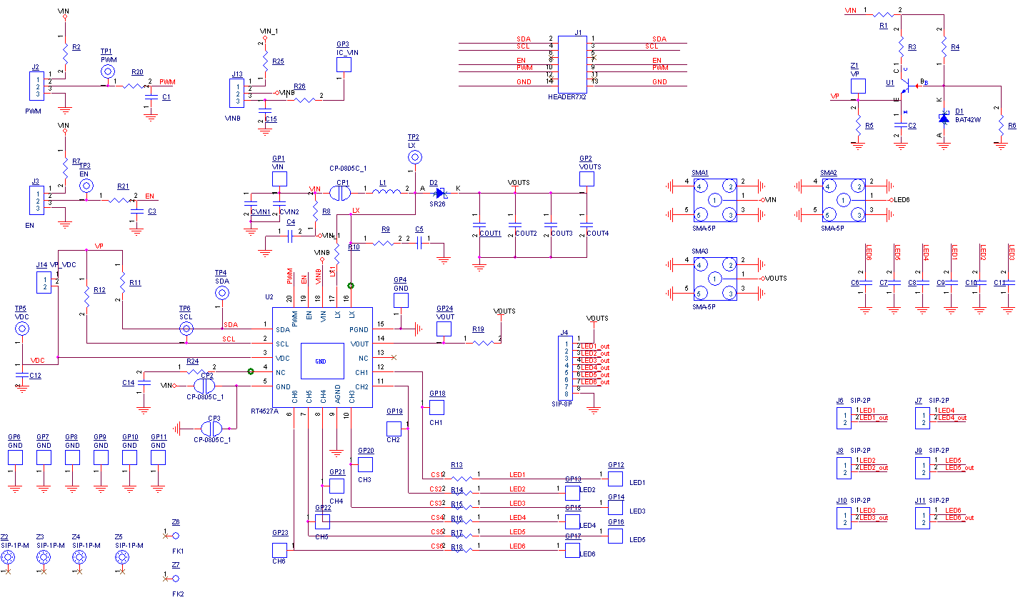
EVB Schematic Diagram
1. The capacitance values of the input and output capacitors will influence the input and output voltage ripple.
2. MLCC capacitors have degrading capacitance at DC bias voltage, and especially smaller size MLCC capacitors will have much lower capacitance.
Measure Result
|
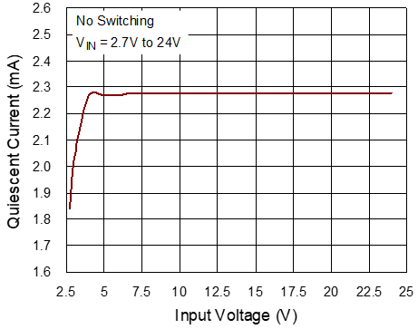
Quiescent Current vs. Input Voltage
|
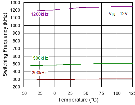
Switching Frequency vs. Temperature
|
|
|
|
|
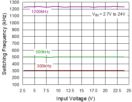
Switching Frequency vs. Input Voltage
|
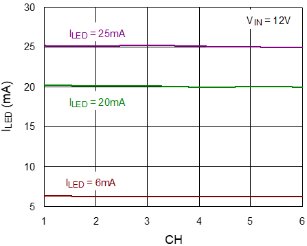
Channel Output Current vs. CHx
|
|
|
|
|
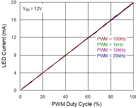
LED Current vs. PWM Duty_ PWM Mode
|
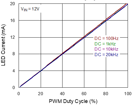
LED Current vs. PWM Duty_ DC Mode
|
|
|
|
|
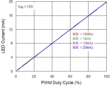
LED Current vs. PWM Duty_ MIX Mode
|
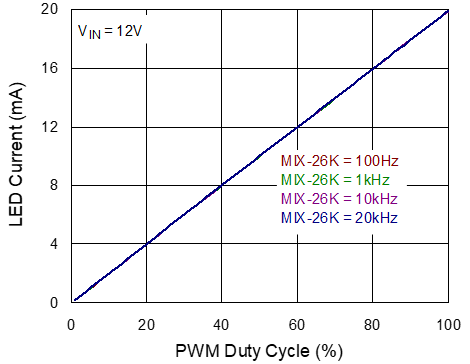
LED Current vs. PWM Duty_ MIX-26K Mode
|
|
|
|
|
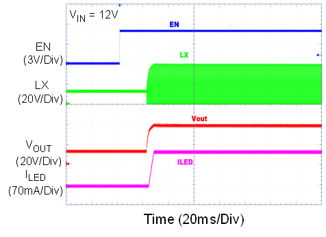
Power On from EN
|
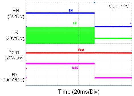
Power Off from EN
|
|
|
|
Evaluation Board Layout
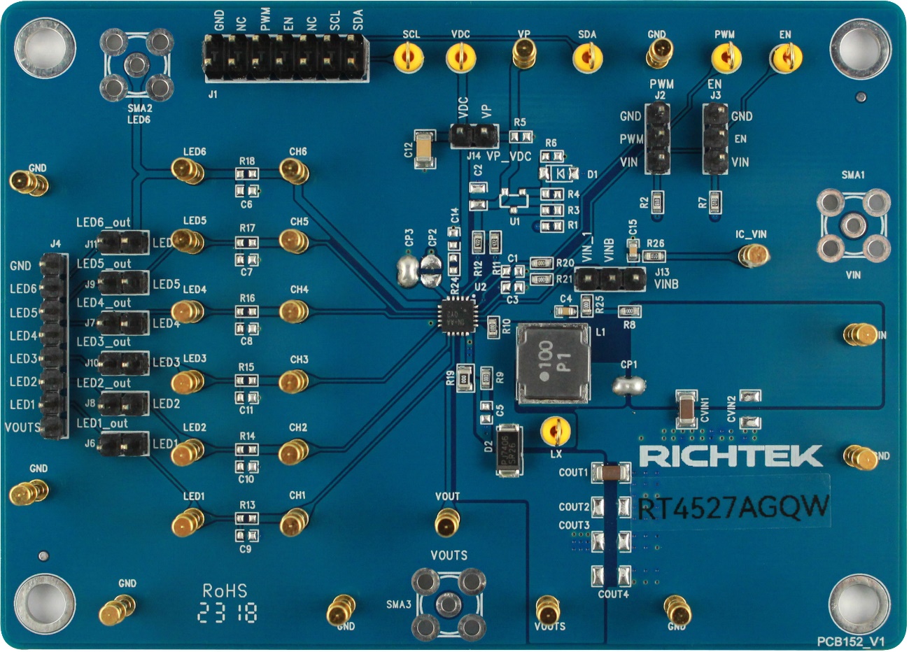
Figure 1 to Figure 4 are RT4527A Evaluation Board layout. This board size is 70mmx50mm and is constructed on four-layer PCB, outer layers with 2 oz. Cu and inner layers with 1 oz. Cu.
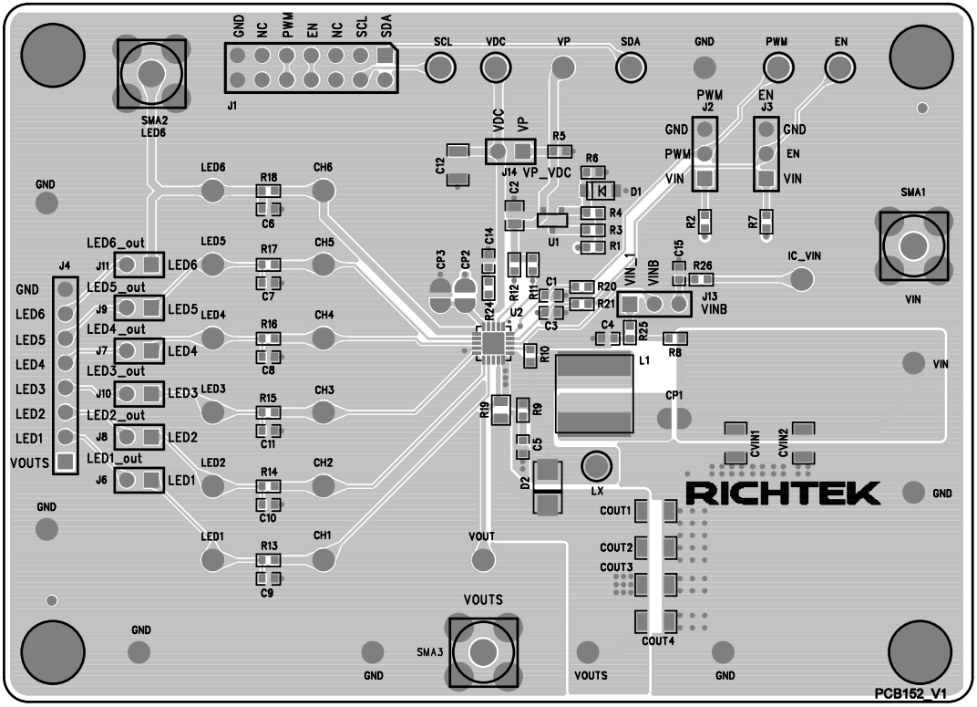
Figure 1. Top View (1st layer)
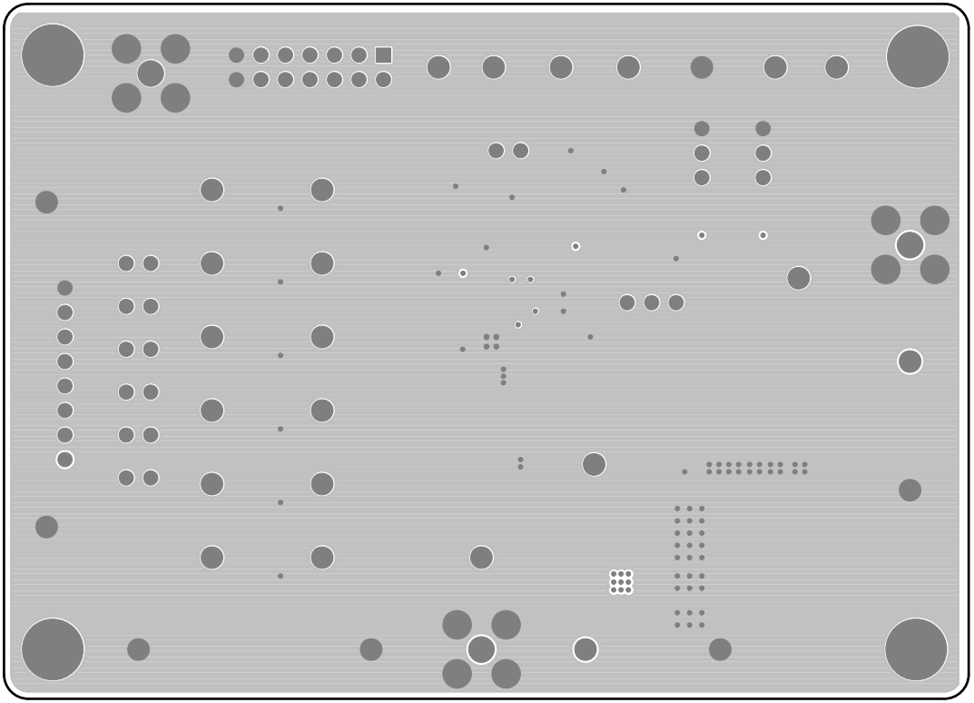
Figure 2. PCB Layout—Inner Side (2nd Layer)
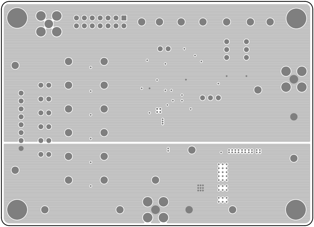
Figure 3. PCB Layout—Inner Side (3rd Layer)
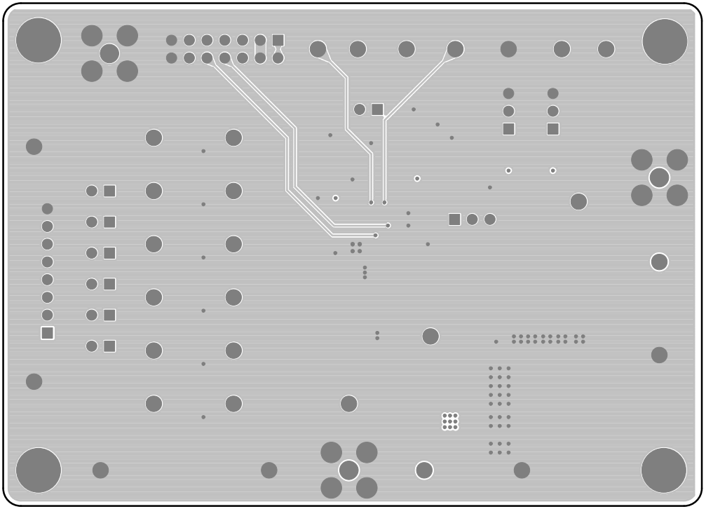
Figure 4. Bottom View (4th Layer)